HomeAuthor

kkpcb02 - KKPCB - Page 3 of 15

Taconic TLY-5 PCB Prototype Release: A Reliable Gate-by-Gate Checklist

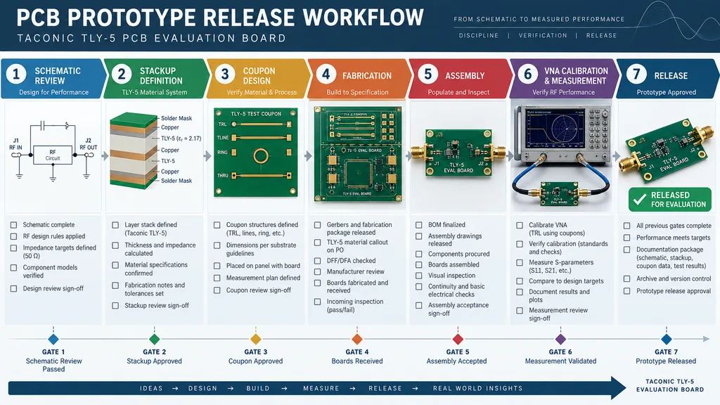
Taconic TLY-5 PCB prototype release is where an RF evaluation board either becomes useful evidence or becomes an expensive collection of assumptions. The design may contain a capable laminate, but the team still needs a finished stackup, launch datum, representative coupon, assembly limits, calibration method, and a clear record of what is typical, calculated, targeted,...
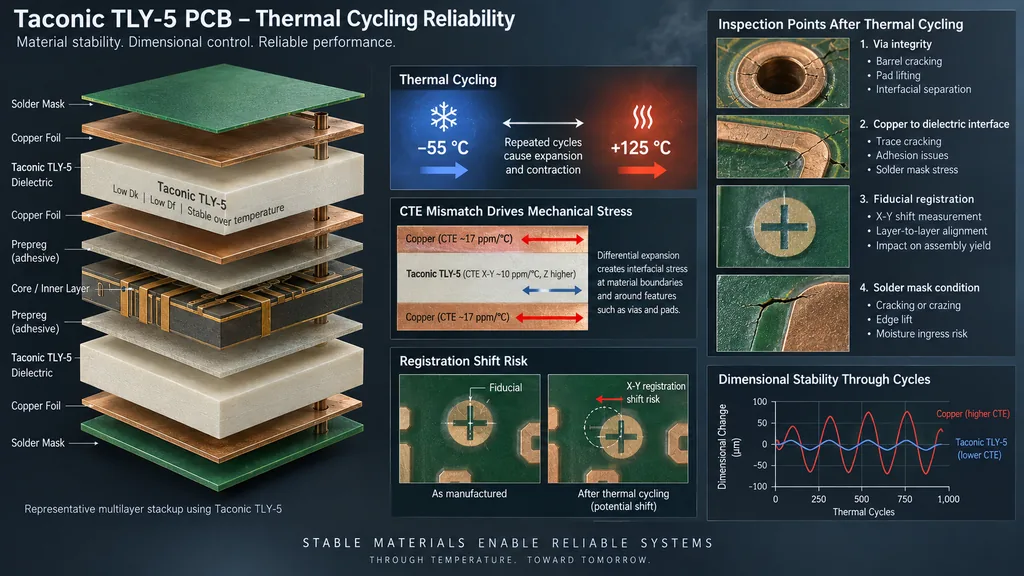
Taconic TLY-5 PCB Thermal Cycling: Reading CTE Mismatch Before It Becomes a Registration Problem

Taconic TLY-5 PCB thermal cycling can expose a registration problem long before a field failure is visible. Different copper, dielectric, mask, connector, and enclosure structures expand at different rates. In a multilayer RF board, that movement can change a via-to-pad relationship, connector datum, or phase-critical line. The right response is to read the CTE path...

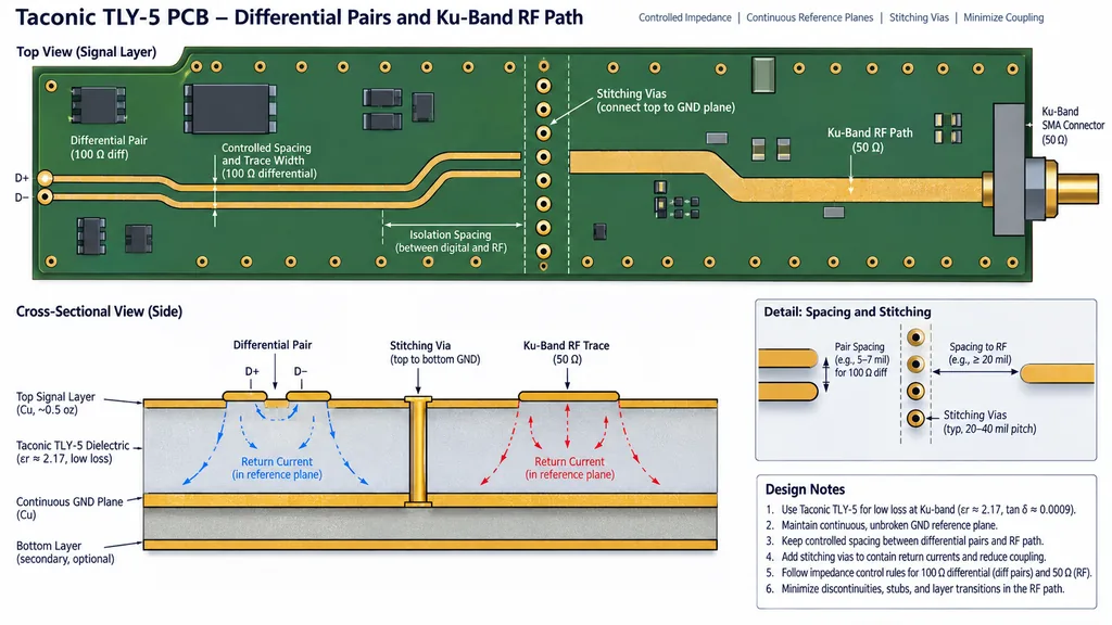
Taconic TLY-5 PCB Differential Pairs: Reliable Reference-Plane Control

Taconic TLY-5 PCB differential pairs on a hybrid RF/digital board need a reference-plane strategy that respects both interfaces. The pair may be electrically balanced in isolation yet experience skew or common-mode conversion when it crosses a split, changes layer, or runs beside a phase-sensitive RF path. The project pain is often discovered at system integration,...

Taconic TLY-5 PCB Solder Mask Strategy: Reliable Open-CPW Decisions at Ku-Band

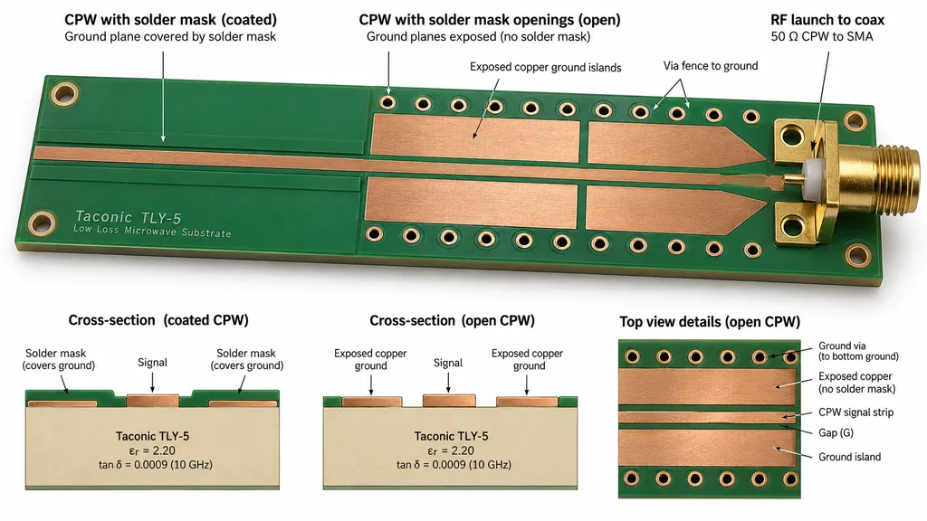
Taconic TLY-5 PCB solder mask decisions can change grounded coplanar waveguide more than a layout review suggests. A blanket coating adds dielectric material above the line, while an open region exposes copper to assembly, handling, and contamination concerns. The correct answer depends on frequency, geometry, finish, process capability, and how the connector or probe references...

Taconic TLY-5 PCB for Ku-Band Satcom: Reliable Feed-Network Layout Decisions

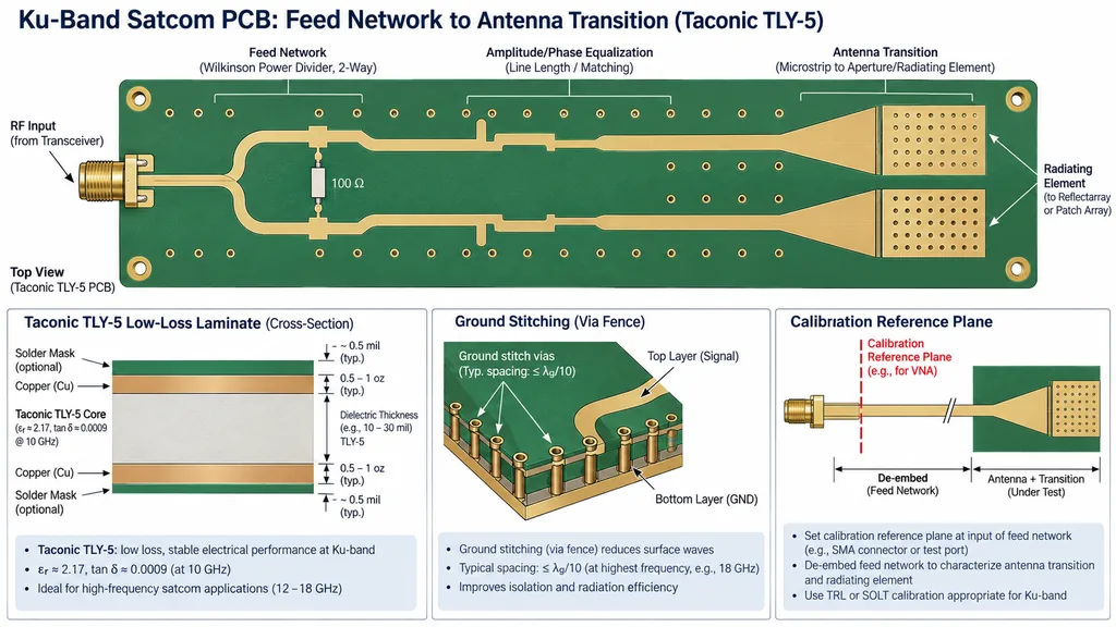
Taconic TLY-5 PCB satcom feed design is won or lost at the interface between the laminate, connector, ground return, and antenna or filter network. A low-loss, low-Dk material can support a compact Ku-band path, but only if the finished stackup and feed datum survive fabrication, assembly, and calibration. The program risk is a feed that...

Taconic RF-35 PCB Rework Limits: Protecting Solder Joints and RF Performance After Assembly

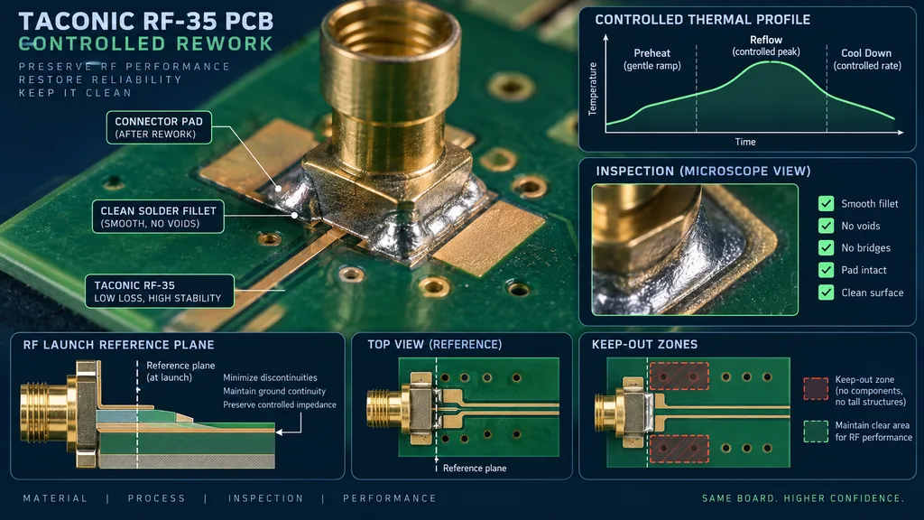
Taconic RF-35 PCB rework limits should be defined before the first failure, not invented at the bench. Removing a connector, amplifier, or shield can change pad adhesion, solder fillet, local copper, and thermal history. On an RF board, those changes may move the launch or reference plane even when the repaired joint looks acceptable under...

Taconic RF-35 PCB for RF Filters: Reliable Coupled-Line Geometry Through Fabrication

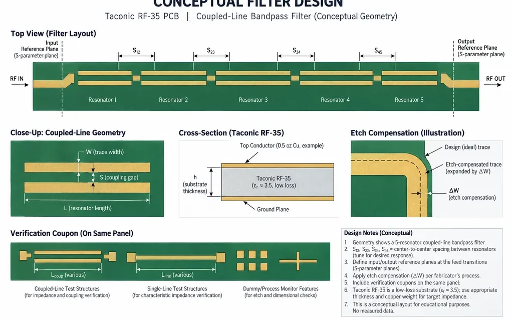
Taconic RF-35 PCB coupled-line filter performance is governed by geometry that fabrication can actually hold. The filter designer may calculate a narrow gap and exact line length, but etch bias, copper profile, dielectric thickness, plating, and solder mask decide whether the finished board has the intended coupling. That is why a filter release needs more...

Taconic RF-35 PCB Surface Finish Choices for Consistent RF Launches

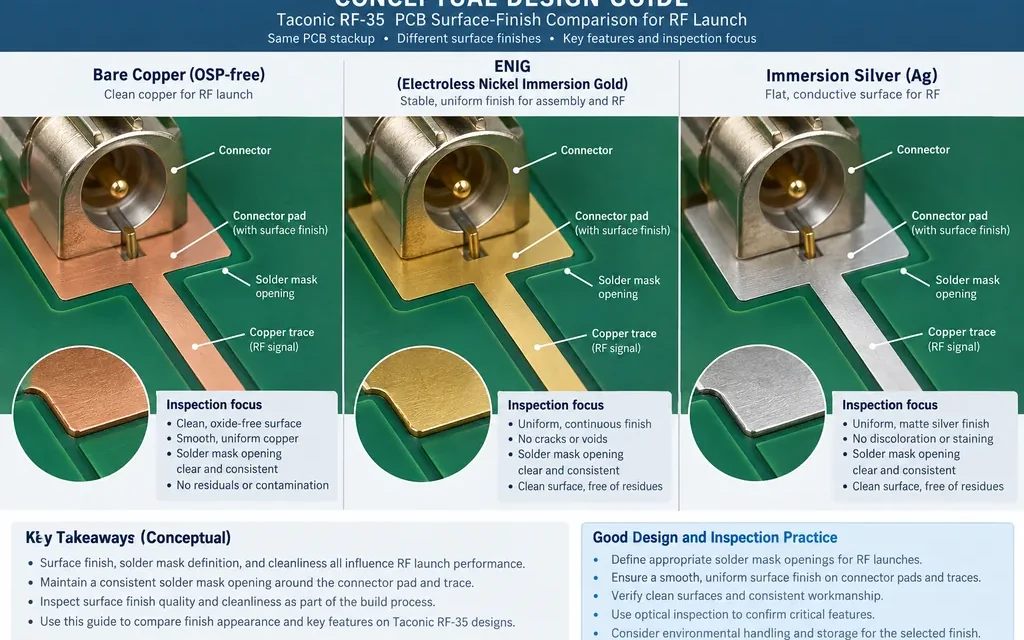
Taconic RF-35 PCB surface finish selection is a launch-interface decision, not a procurement checkbox. A finish changes pad topography, solder wetting, contact behavior, and the geometry the RF current sees at the connector or package transition. The project pain appears when a finish is changed after layout release and the team has no coupon or...

Taconic RF-35 PCB Ground Via Fences: Reliable Coupling Control in Dense Wireless Modules

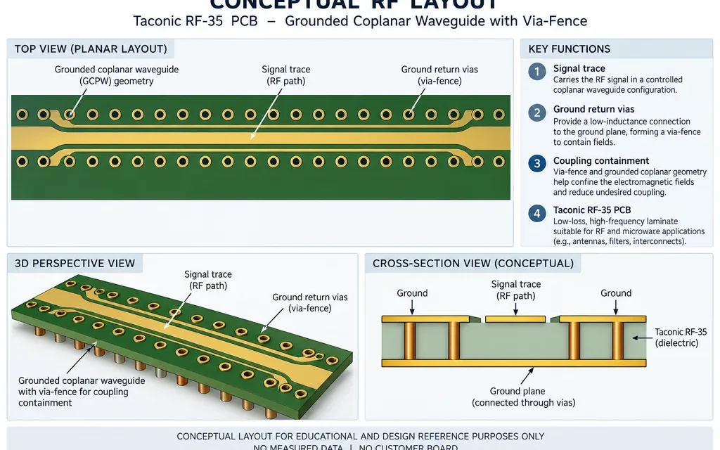
Taconic RF-35 PCB via fence coupling control is a layout-and-fabrication problem. A fence can contain a field only when its pitch, plane connection, anti-pad, and registration match the frequency range and stackup. In a dense wireless module, an apparently complete row can still leak through a split plane, connector keep-out, or drill offset. Table of...

TLY-5 PCB Panelization: A Robust Registration Strategy for RF Assembly

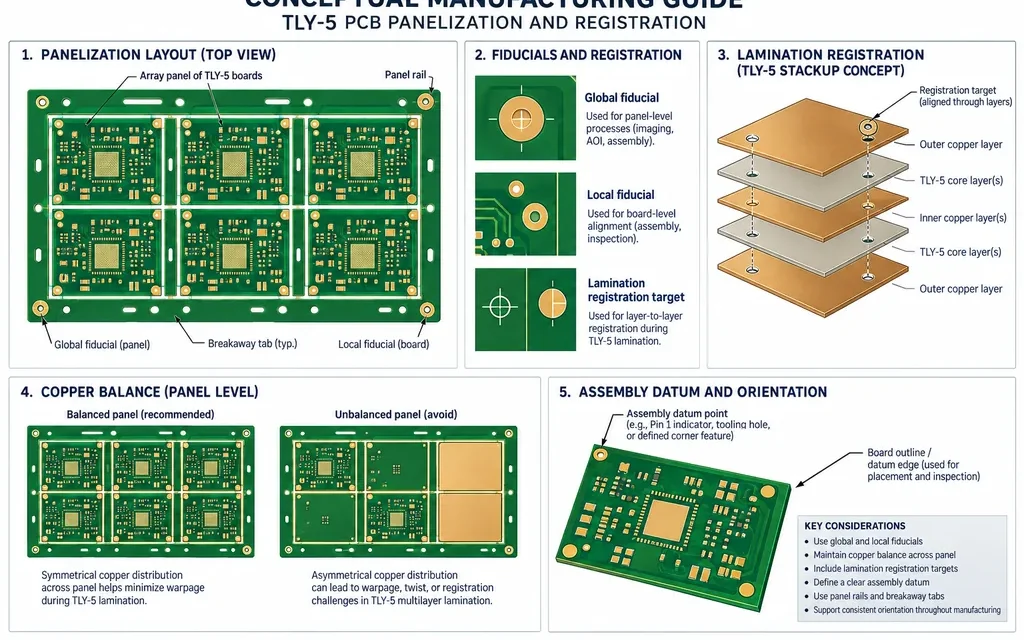
TLY-5 PCB panelization registration is a project risk when a low-Dk RF design is copied into a manufacturing panel without considering press flow, copper distribution, routing, and assembly tooling. The board may be electrically correct as an individual drawing yet lose connector alignment or channel-to-channel phase consistency after it is nested, laminated, routed, and depanelized....