HomeTag

low-loss PCB - KKPCB

Assembly Controls for an Automotive High Frequency PCB Under Thermal Stress

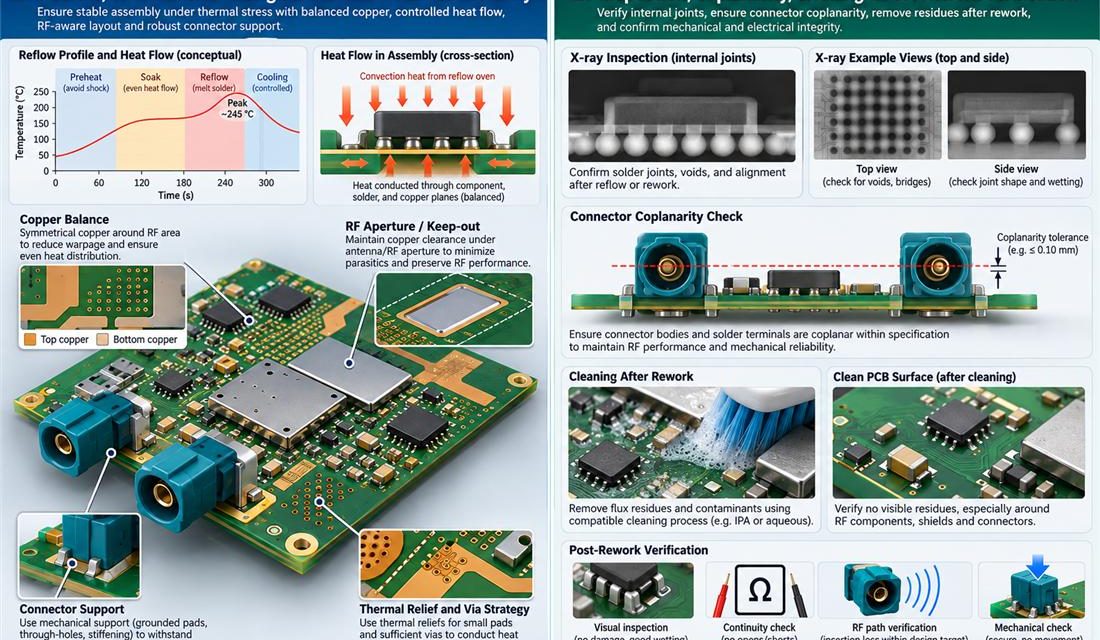
Automotive High Frequency PCB — Fabrication can meet a drawing and assembly can still move the electrical result. Paste height, reflow warpage, shield force, cleaning chemistry, heat spreaders, and connector rework all act on high-frequency automotive radar and connectivity boards where fast edges, 76–81 GHz channels, and a constrained metal housing share the same release....

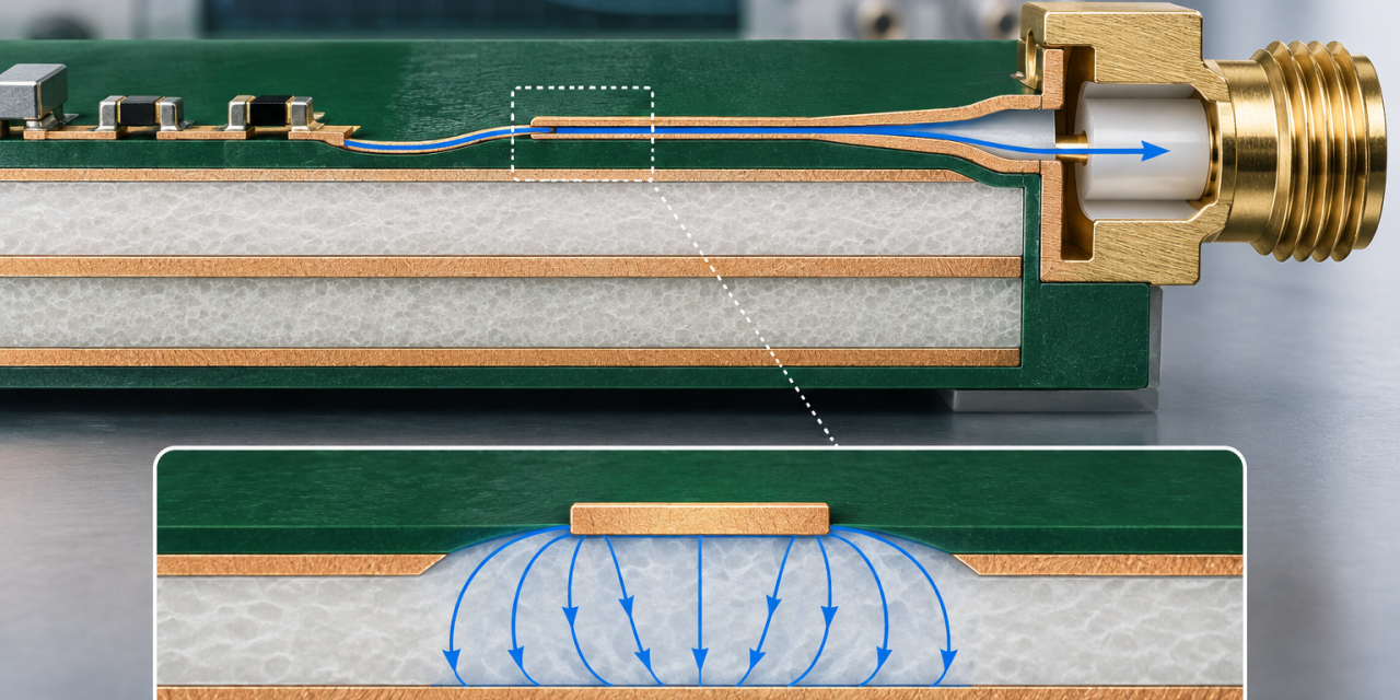
Designing the Connector Launch of an Automotive High Frequency PCB

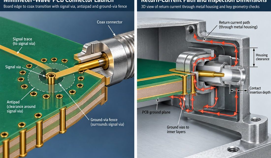
Automotive High Frequency PCB — The connector, coax, antenna, sensor flex, or board edge is where a schematic becomes a three-dimensional part. In high-frequency automotive radar and connectivity boards where fast edges, 76–81 GHz channels, and a constrained metal housing share the same release, that interface also has to survive mating force, housing tolerances, and...

Finding the Physical Cause of Drift in an Automotive High Frequency PCB

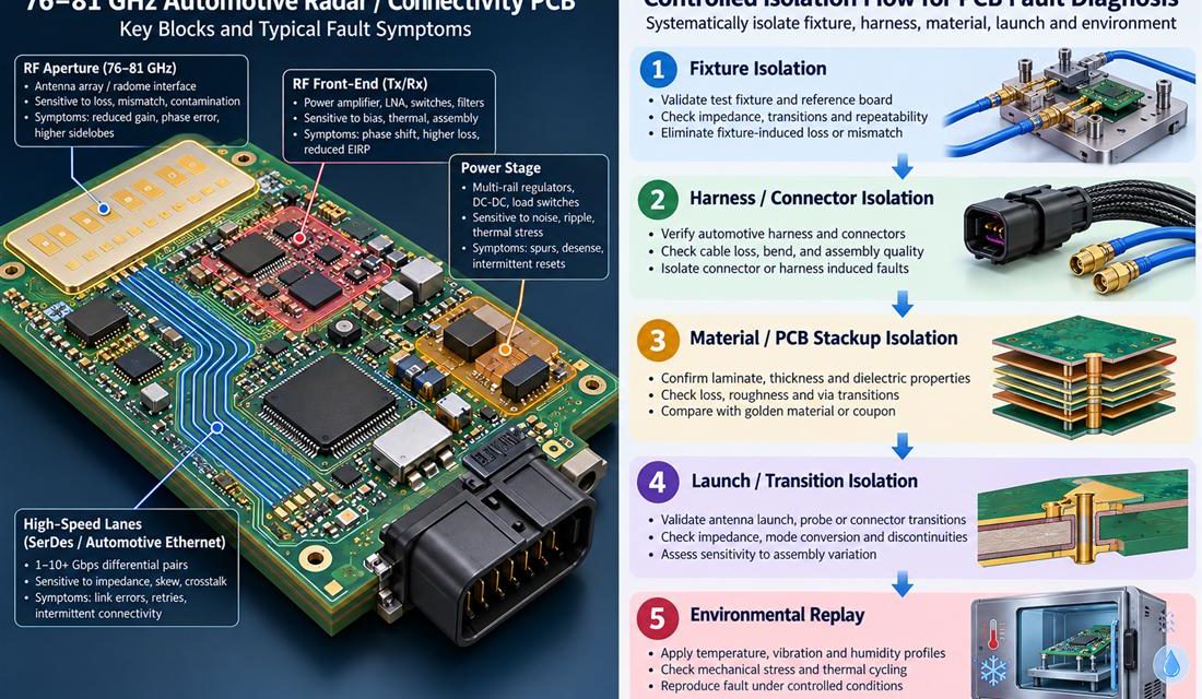
Automotive High Frequency PCB — A vehicle program can report an intermittent reset, a communication dropout, a radar sensitivity loss, or a calibration value that moves only after the enclosure is closed. That symptom is not yet a PCB diagnosis. On a Automotive High Frequency PCB, the board shares its boundary with a harness, connector,...

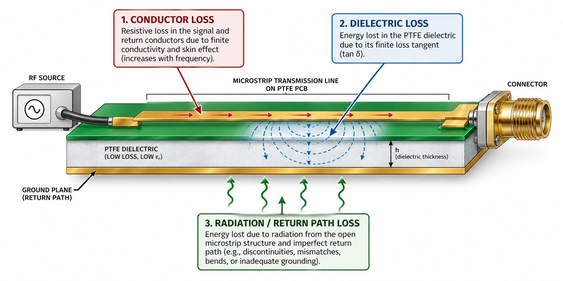
PTFE PCB Loss Budgets: Copper Profile Checks for Long RF Paths

When a microwave path becomes long enough, the material name alone cannot explain insertion loss. A PTFE PCB combines dielectric loss, conductor roughness, trace geometry, resin or ceramic loading, connector transitions, and the return path. Engineers often discover the real problem during a system margin review because the original estimate used a catalog loss tangent...

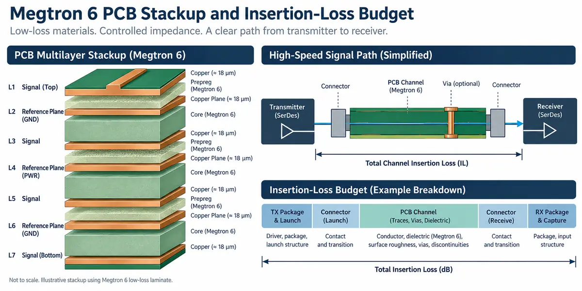
Megtron 6 PCB Material Selection: Turning Loss Budgets into a Manufacturable Stackup

Megtron 6 PCB projects often fail late for a simple reason: the electrical loss budget was written before the stackup, copper profile, and connector geometry were frozen. A material family can support demanding high-speed channels, but the released board still depends on resin content, finished dielectric thickness, reference-plane continuity, copper roughness, and fabrication capability. This...

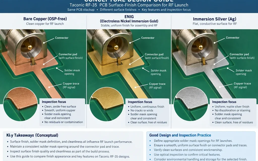
Taconic RF-35 PCB Copper Roughness: Turning Conductor Loss Into a Release Check

Table of Contents Copper profile and loss budget Drawing notes and finished geometry Cross-section inspection Procurement release gate Taconic RF-35 PCB projects often pass a schematic review and still lose margin at the first production build. The hidden variable is frequently conductor loss: copper roughness, finished trace width, etch shape, and the way the reference...

Duroid 5880 PCB Stackup: 7 Critical Controls for Low-Loss RF Fabrication

Microwave design teams often choose Duroid 5880 for its low-loss behavior, then discover that stackup translation and fabrication details decide whether the finished board matches the model. A production-ready Duroid 5880 PCB needs a controlled dielectric reference, consistent copper geometry, and inspection points that survive panel processing. This guide turns those requirements into a practical...

Double Layer HF PCB: High-Frequency Two-Layer PCB Solutions for RF and Microwave Applications

Why Double Layer HF PCB Technology Is Important Modern wireless communication systems continue evolving toward: Higher operating frequencies Faster wireless transmission Compact RF module integration Low-loss microwave communication Miniaturized antenna systems Applications such as: RF communication modules IoT wireless devices Automotive radar sensors 5G communication systems Microwave antenna platforms require PCB solutions capable of delivering:...