
The Ultrasound PCB ADC LVDS interface is the handoff where quiet echo capture becomes a high-speed data problem. Moving digitized echo data off an ultrasound front end is not a simple “place the converter and route the bus” task. The analog receive chain is trying to preserve microvolt-level information while an ADC clock, LVDS serializer, memory interface, and processor are creating fast return currents nearby. A board can pass a schematic review and still lose usable dynamic range because the clock return path crosses a power split, the LVDS escape cuts through a quiet analog corridor, or the stack-up supplied to fabrication does not match the impedance assumptions used by the layout team.
That makes the Ultrasound PCB ADC LVDS interface a release problem as much as a routing problem. The handoff needs an explicit reference plane, a defined layer transition, and an inspection point for each fast corridor.
This guide treats the Ultrasound PCB ADC LVDS interface as a mixed-signal boundary. It treats an Ultrasound PCB as a mixed-signal measurement platform. It shows how to release an ADC/LVDS interface as a coordinated electrical, mechanical, and manufacturing package. The examples are engineering design targets rather than claimed customer measurements. Where a value depends on the converter, transducer, or cable, the correct practice is to confirm it with the component data sheet and the final controlled-impedance coupon.
- Give every signal corridor an owner
- Build the stack-up around return current
- Route LVDS and clocks as a coupled system
- Turn the design into a production release
- Verify the handoff before the first panel
Give every signal corridor an owner before routing
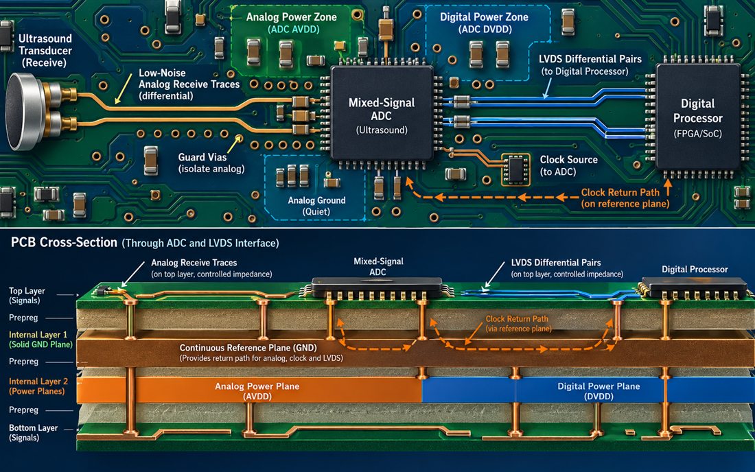
The first project failure usually occurs before a trace is drawn. The analog front end, converter, clock source, LVDS receiver, and connector are assigned to different engineers, so each group optimizes its own block. The result is a board with no agreed current map. A better PCB design review marks four corridors on the floorplan: the transducer and low-noise receive path, the ADC sampling and reference network, the clock distribution path, and the digital egress. Each corridor gets a reference plane, an allowed via strategy, and a keep-out rule.
For the receive corridor, keep the input network compact and make the return path continuous under every differential pair and filter section. The ADC reference pins deserve their own quiet island only when the island still has a controlled connection to the intended analog ground. An isolated copper island with a long neck is not automatically quiet; it can become an antenna for the clock edge. Use the PCB materials decision to control dielectric thickness and loss before changing trace geometry. That keeps the stack-up discussion tied to the actual signal bandwidth instead of to a generic four-layer recipe.
Decide which noise mechanism is being controlled
Engineers often describe every problem as “EMI.” For this interface, separate the mechanisms. Capacitive coupling is reduced by spacing, a grounded guard, and a stable reference plane. Inductive coupling is reduced by minimizing loop area and keeping the return current directly below the aggressor. Simultaneous-switching noise is controlled by low-inductance decoupling and short power loops. Connector or cable radiation is controlled by a defined launch, shield termination, and chassis strategy. Writing the mechanism beside each layout rule prevents a late review from adding random copper that does not solve the observed path.
Build the Ultrasound PCB stack-up around return current
The Ultrasound PCB ADC LVDS interface is sensitive to the order in which layers, planes, and component references are released. An Ultrasound PCB ADC/LVDS ultrasound board normally benefits from a continuous reference plane directly adjacent to the high-speed signal layer. The exact dielectric thickness, copper weight, and trace width for the Ultrasound PCB ADC LVDS interface must be calculated from the fabricator’s controlled stack-up, not copied from a simulator’s default.
For a multilayer build, ask the manufacturer to return the proposed layer arrangement with finished dielectric values, copper thickness after plating, and the test-coupon geometry. A controlled multilayer PCB stack-up lets the analog pair, clock, and LVDS pair share a predictable return environment without forcing them onto the same physical corridor.
| Interface | Primary risk | Release control |
|---|---|---|
| Transducer to AFE | Input capacitance and external noise | Short differential route, guard strategy, clean reference |
| ADC sample clock | Return-current injection into the AFE | Continuous plane, local decoupling, no split crossing |
| ADC to LVDS | Pair skew and via discontinuity | Matched escape, identical layer transitions, impedance target |
| LVDS to connector | Common-mode conversion | Symmetric launch, ground stitching, mechanical datum |
Do not route a clock over a plane boundary simply because the boundary is “only” between analog and digital power. The return current follows the lowest-inductance path available at the edge rate, which may be a long detour through stitching capacitors or connector grounds. If a plane split is unavoidable, define a short bridge and place the bridge components before routing. This is one reason a PCB manufacturing review should happen while the stack-up is still negotiable: the fabricator can identify whether a plane void, back-drill, or via-in-pad rule will change the assumed return path.
Keep the converter reference network physically quiet
Place reference capacitors, the analog supply bead, and the converter ground pins in one compact loop. The loop should not share a neck with the LVDS fanout. If the package requires thermal vias, make their connection to the reference plane intentional and check that the via field does not pierce an adjacent differential pair. The most robust high-frequency PCB practice is to reserve the reference plane first, then fit the copper pour around that decision instead of pouring copper and assuming the return is continuous.
Route LVDS and clocks as a coupled system
The Ultrasound PCB ADC LVDS interface must be reviewed as one electrical corridor. LVDS is differential, but it is not immune to a bad reference. Treat the pair, its return current, the clock source, and the receiving connector as one system. Keep pair spacing consistent through the BGA or QFN escape; avoid an abrupt neck-down on one side; and use the same number of vias on both conductors when a layer transition is required. If the pair must move around a keep-out, bend both traces together and preserve the local reference. A short, symmetric PCB assembly launch is easier to inspect and rework than a pair that disappears under a connector body.
Clock routing needs an even stricter rule. In an Ultrasound PCB ADC LVDS interface, the clock return must remain predictable even when the digital processor changes lane timing. The clock should enter the ADC with a clean reference and should not share a via field with the receive input.
Place its series damping component at the source when the driver data sheet supports that arrangement. Keep the clock return in the same plane through the converter escape. The digital processor may tolerate a few picoseconds of additional skew; the analog front end may not tolerate the corresponding current spike. This is why the project timing plan should reserve an impedance review before the first schematic freeze, not after the prototype is already built.
For long LVDS runs, define the pair impedance for the Ultrasound PCB ADC LVDS interface and termination assumptions in the fabrication notes. A generic “100 ohm differential” note is incomplete if the stack-up, solder-mask assumption, test coupon, and allowable skew are missing. Use the RF PCB and controlled-impedance PCB manufacturing conversations to make the test method explicit. If the exact page is not available in the active site, replace it with the verified PCB layout page rather than leaving a dead link.
Turn the design into a production release
The design is not ready when the traces look clean. A high-reliability Ultrasound PCB release makes the inspection intent visible to fabrication and assembly. A reliable Ultrasound PCB ADC LVDS interface release makes the inspection intent visible to fabrication and assembly. It is ready when another engineer can rebuild the electrical assumptions from the release package. Include the approved stack-up, impedance table, layer-to-layer transition rules, via fill or back-drill requirements, solder-mask expansion, component courtyard, and probe-access notes. Add a drawing that identifies the ADC datum, connector datum, and the test-coupon location. The manufacturing team can then compare the board’s critical geometry to the actual panel process instead of inferring requirements from a screenshot.
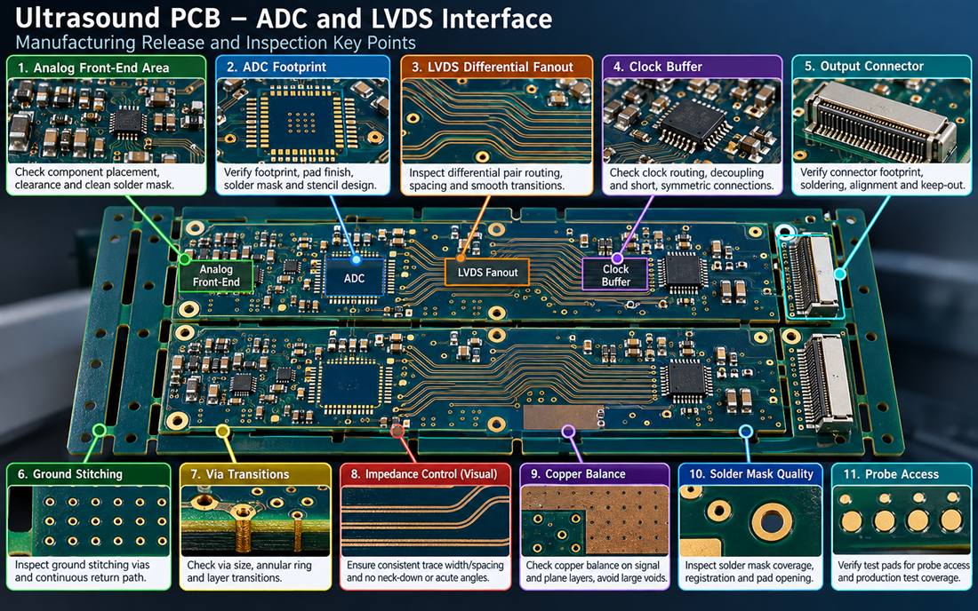
Assembly risk is often hidden in the interface between the ADC footprint and its thermal pad. Confirm stencil aperture rules, paste reduction, voiding expectations, and optical-inspection access. For the LVDS connector, define coplanarity, keep-out, solder fillet, and mechanical datum together. A production PCB prototype should use the same connector launch and coupon method planned for the release build; otherwise the prototype only proves that the board can be assembled, not that the interface is repeatable.
Use a change-control gate for every interface edit
When a supplier changes dielectric thickness, a connector changes pin pitch, or firmware changes the lane order, require a short impact review. The review should identify whether the change affects pair length, plane continuity, power integrity, thermal relief, or probe coverage. Record the answer beside the revision, not only in an email thread. This turns PCB fabrication feedback into a controlled engineering decision and protects the project manager from approving a “minor” change that moves the ADC clock across the receive return path.
Verify the Ultrasound PCB handoff before the first panel
A practical pre-release check for a Ultrasound PCB has five passes. First, compare the component placement to the signal-corridor map. Second, inspect every clock and LVDS via transition for a continuous reference. Third, compare the impedance table to the fabricator’s finished stack-up and coupon. Fourth, inspect the assembly drawing for probe access, stencil constraints, and connector datum. Fifth, review the revision package with the test engineer so the intended observation points exist on the physical board. If a requirement cannot be inspected, it is not yet a release requirement.
For the first build, separate design targets from measured evidence. The release package for the Ultrasound PCB ADC LVDS interface should identify each target and its owner. The Ultrasound PCB ADC LVDS interface should carry those targets into the inspection plan. A target such as “maintain the specified differential impedance through the connector launch” is valid before fabrication; a claim about insertion loss or ADC noise requires the actual coupon or board measurement. That distinction keeps the PCB testing plan credible and gives the project team a clear decision when a result falls outside the expected range. The same package can then be reused for a controlled PCBA build without rewriting the interface rules.
For engineers, the key lesson is to release the return path of the Ultrasound PCB ADC LVDS interface and inspection method as deliberately as the signal trace. For project managers, the key lesson is that stack-up approval, connector selection, and DFM review are dependencies, not paperwork. When those dependencies are closed before fabrication, an Ultrasound PCB can move from analog capture to digital processing without turning the ADC/LVDS boundary into the next unexplained noise source.
A documented Ultrasound PCB ADC LVDS interface lets the next revision reuse the same stack-up, test points, and inspection logic without copying an old board blindly.
The Ultrasound PCB ADC LVDS interface release should carry the same stack-up assumptions into procurement, assembly, and inspection. Treat the Ultrasound PCB ADC LVDS interface as one controlled feature, and keep its Ultrasound PCB ADC LVDS interface checklist with the revision package.
Sources: component data sheets and application notes for the selected ADC, clock source, LVDS interface, and connector; material and fabrication data supplied for the approved stack-up; and engineering guidance from Analog Devices, Qorvo, Würth Elektronik, and relevant RF/PCB manufacturing references. Values in this article are design targets or engineering ranges, not customer measurement claims.
