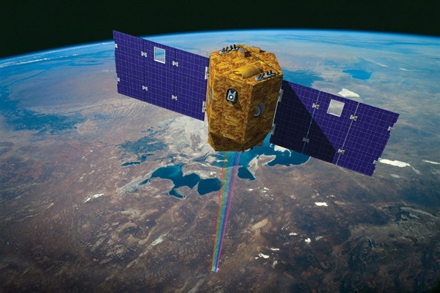
signal integrity PCB - KKPCB
 
HomeTag

signal integrity PCB - KKPCB

High Speed PCB: Advanced PCB Design for High-Frequency and High-Speed Signal Transmission

1. Why High Speed PCB Technology Is Essential Modern electronic systems are evolving rapidly toward: Faster data transmission rates Higher operating frequencies Greater circuit integration density AI-driven computing platforms High-bandwidth communication systems Applications such as: 5G infrastructure AI servers Data centers High-performance computing Automotive radar systems High-speed networking equipment require PCB designs capable of maintaining...

Buried Via PCB: Advanced Multilayer PCB Technology for High-Density Interconnection Design

1. Why Buried Via PCB Technology Is Essential for Modern Electronics As modern electronic products continue evolving toward: Smaller device size Higher circuit density Faster signal transmission More complex multilayer PCB structures traditional through-hole PCB technology is increasingly limited in: Routing space Signal integrity High-speed PCB performance Component density To overcome these limitations, manufacturers increasingly...

Low Dissipation Factor PCB: High-Speed and High-Frequency PCB Solutions for Low Signal Loss Applications

1. Why Low Dissipation Factor PCB Is Critical in Modern Electronics As modern electronic systems continue advancing toward: Higher operating frequencies Faster data transmission speeds Greater signal density More compact RF modules PCB materials play a critical role in determining: Signal transmission quality RF efficiency High-speed communication stability In applications such as: 5G and 6G...

Low Loss PCB: Materials, Design Principles, and High-Frequency Performance Optimization

1. Introduction: Why Low Loss PCB Is Essential in Modern Electronics As electronic systems evolve toward: Higher data rates Higher operating frequencies Increased signal density Greater system integration traditional PCB materials such as standard FR4 are no longer sufficient for advanced RF and high-speed applications. In modern systems including: 5G/6G communication networks Automotive radar systems...

1. Introduction to Impedance Controlled PCB As modern electronic systems continue advancing toward: Higher frequencies Faster data transmission Higher signal density traditional PCB routing methods are no longer sufficient to guarantee stable signal transmission. In applications such as: 5G communication systems High-speed servers Automotive radar RF and microwave electronics Aerospace communication systems Impedance Controlled PCB...

Impedance Controlled PCB: Precision Solutions for High-Speed & RF Signal Integrity

What is an Impedance Controlled PCB? An Impedance Controlled PCB is a printed circuit board designed and manufactured to maintain a specific characteristic impedance for signal traces, ensuring consistent signal transmission. In high-speed and RF designs, the PCB trace behaves like a transmission line. Without proper impedance control, signals can suffer from reflection, distortion, and...

Low Loss PCB: High-Speed & High-Frequency Solutions for Signal Integrity Optimization

What is a Low Loss PCB? A Low Loss PCB is a printed circuit board designed using materials and structures that minimize signal attenuation (loss) during transmission, especially in high-frequency and high-speed applications. As data rates and frequencies increase, signal loss becomes a critical issue. Standard PCB materials like FR4 introduce higher dielectric loss, making...

RF Trace PCB: Design Guidelines for Controlled Impedance & High-Frequency Signal Integrity

What is an RF Trace PCB? An RF Trace PCB refers to a printed circuit board specifically designed with controlled impedance traces to handle radio frequency (RF) signals. Unlike standard PCB routing, RF traces must maintain consistent electrical characteristics to avoid signal loss, reflection, and distortion. In RF design, the trace itself becomes part of...

Logic Test PCB: Designing High-Speed Digital Test Platforms for Accurate Validation

What Is a Logic Test PCB? A Logic Test PCB is a specialized digital test PCB used to verify the functionality, timing, and performance of digital ICs and high-speed logic devices. Unlike standard circuit boards, a Logic Test PCB is designed as part of an ATE PCB system, where accurate signal delivery and measurement are...

RF Trace PCB Design: Optimizing High-Frequency Signal Paths for Maximum Performance

What Is an RF Trace PCB? An RF Trace PCB is a specialized RF PCB where signal routing is designed as controlled transmission lines to carry high-frequency signals with minimal loss and distortion. In RF Trace PCB design, traces are no longer simple connections—they function as engineered RF signal paths, where geometry, materials, and layout...