HomeTag

5G PCB - KKPCB

From EVT Evidence to Volume Release for a 5G Module PCB

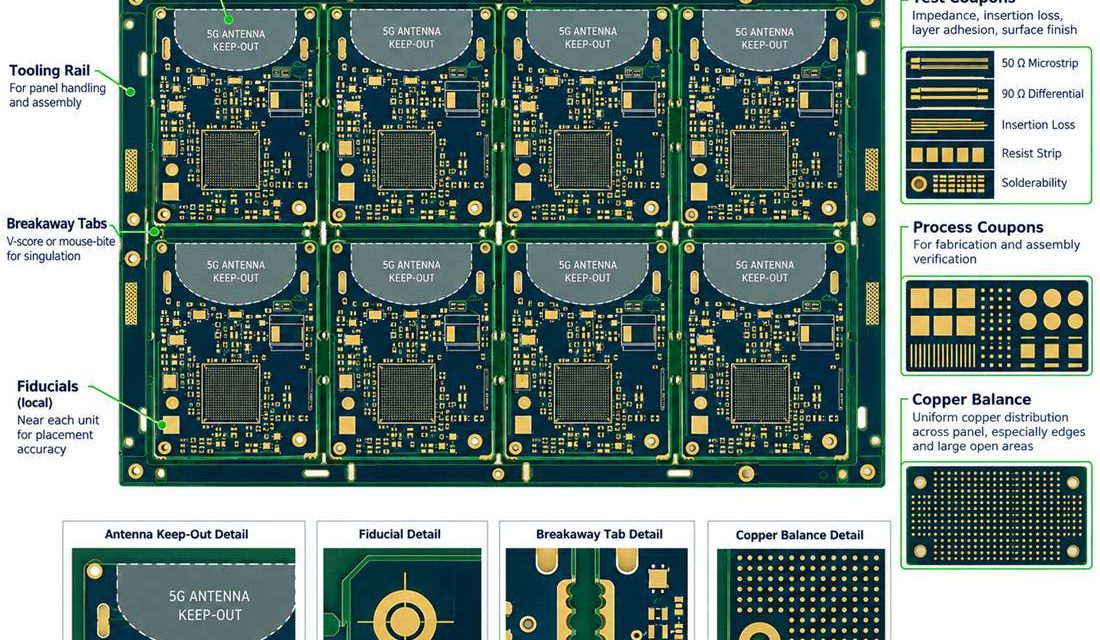
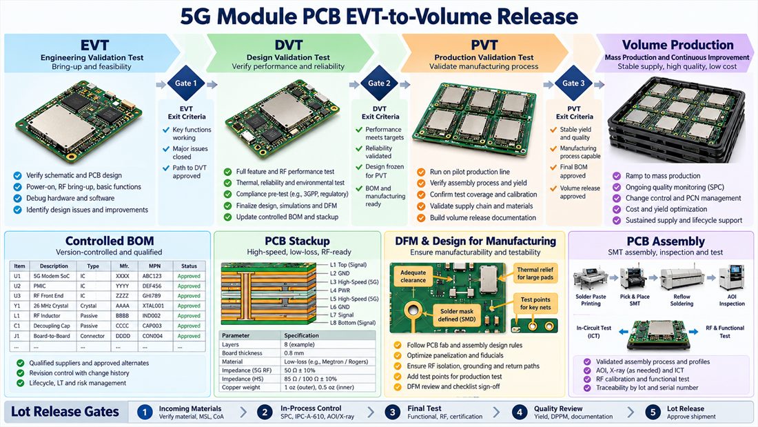
5G module PCB production release begins when design evidence, supplier capability, and change control agree. The last ten percent of a board program is rarely a single design change. It is the point where a prototype stackup, a supplier process, a connector choice, and an enclosure must become one controlled release. For compact radio modules...
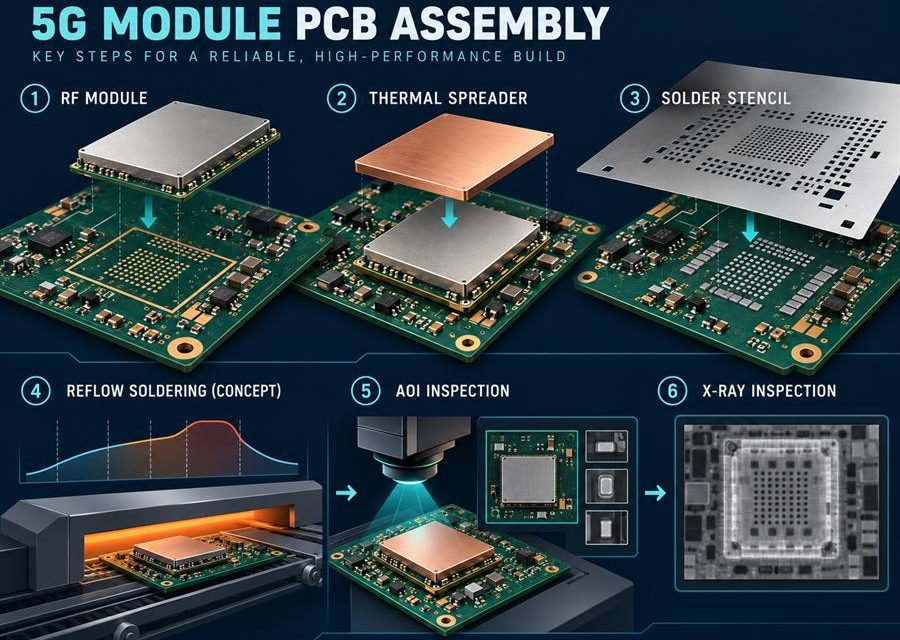
Keeping RF Performance Intact Through 5G Module PCB Assembly

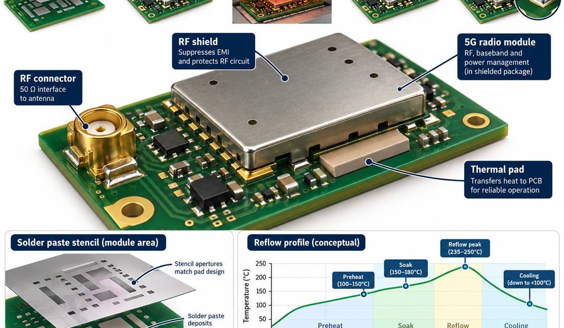
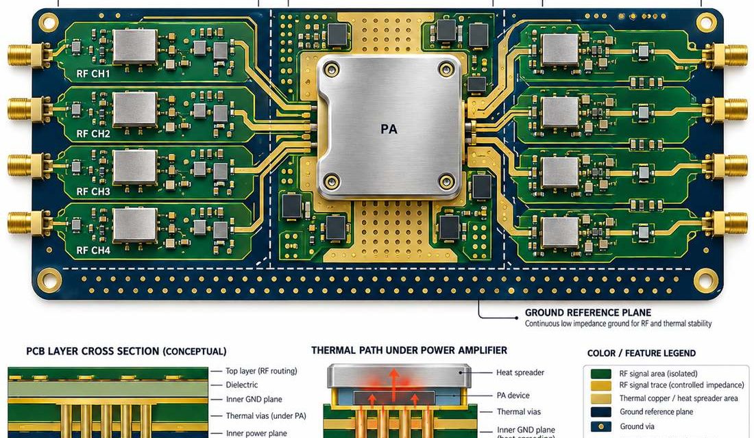
5G module PCB assembly release begins by treating heat, solder, cleaning, and mechanical force as RF variables. An RF board can leave fabrication within drawing limits and still change during paste printing, reflow, shielding, cleaning, or mechanical assembly. That risk is amplified in compact radio modules used in private 5G radios, fixed-wireless units, and edge...

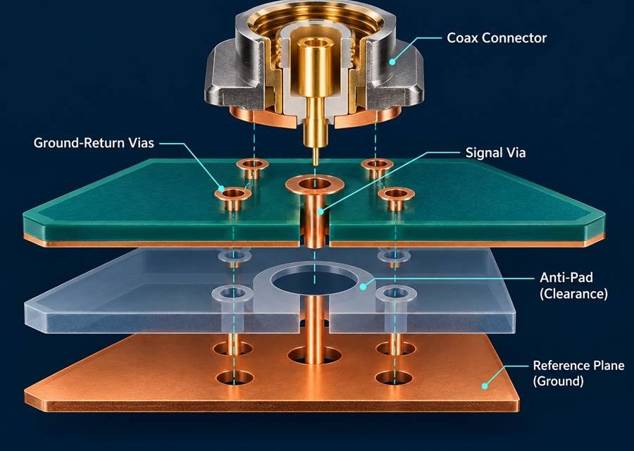
Designing Connector and Via Transitions for a 5G Module PCB Launch

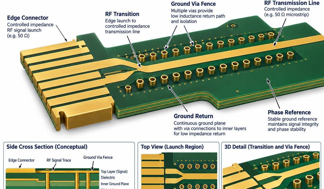
5G module PCB launch design begins with a complete three-dimensional signal and return path. The boundary between a board and a connector, coax, antenna, or shield is where a clean schematic becomes a three-dimensional electromagnetic problem. In compact radio modules used in private 5G radios, fixed-wireless units, and edge gateways, that boundary can set the...

Selecting a 5G Module PCB Stackup Without Hiding the Loss Budget

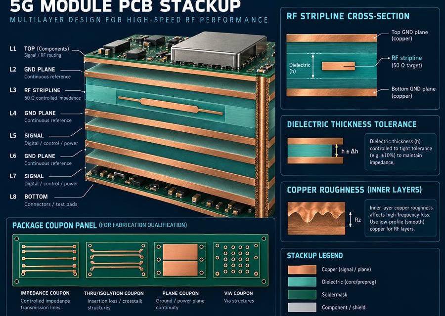
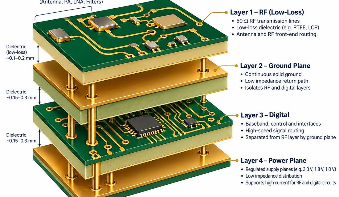
5G module PCB stackup release begins by making every electromagnetic and manufacturing assumption visible. Stackup discussions fail when the drawing lists layer names but not the electromagnetic and manufacturing assumptions behind them. In compact radio modules used in private 5G radios, fixed-wireless units, and edge gateways, the board must carry RF energy, power current, high-speed...

5G PCB DFM Release: 5 Production Checks

When a team selects 5G PCB, it is usually solving a specific product constraint rather than buying a label. This article takes a dfm view of 5G radio-board material choices, copper geometry, controlled references, and power-to-RF partitioning. The project pain is phase drift, insertion-loss budget, thermal coupling from power amplifiers, and a stack -up that...

5G PCB Assembly: 5 Reliability Controls

When a team selects 5G PCB, it is usually solving a specific product constraint rather than buying a label. This article takes a assembly view of 5G radio-board material choices, copper geometry, controlled references, and power-to-RF partitioning. The project pain is phase drift, insertion-loss budget, thermal coupling from power amplifiers, and a stac k-up that...

5G PCB Via Launch: 5 Transition Checks

When a team selects 5G PCB, it is usually solving a specific product constraint rather than buying a label. This article takes a transition view of 5G radio-board material choices, copper geometry, controlled references, and power-to-RF partitioning. The project pain is phase drift, insertion-loss budget, thermal coupling from power amplifiers, and a stack-up that changes...

5G PCB Stack-Up: 5 Geometry Controls

When a team selects 5G PCB, it is usually solving a specific product constraint rather than buying a label. This article takes a stackup view of 5G radio-board material choices, copper geometry, controlled references, and power-to-RF partitioning. The project pain is phase drift, insertion-loss budget, thermal coupling from power amplifiers, and a stack-u p that...

5G PCB Thermal Path: 5 Release Checks

When a team selects 5G PCB, it is usually solving a specific product constraint rather than buying a label. This article takes a thermal view of 5G radio-board material choices, copper geometry, controlled references, and power-to-RF partitioning. The project pain is phase drift, insertion-loss budget, thermal coupling from power amplifiers, and a s tack-up that...

RO4350B PCB Stackup Selection for 5G and Microwave Mixed-Signal Boards

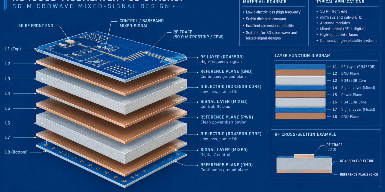
When a radio board combines a 5G front end, clock distribution, and digital processing, stackup selection becomes a system decision rather than a material shortcut. An RO4350B PCB can provide a predictable RF foundation, but only when the chosen dielectric thickness, copper, reference planes, and mixed-signal boundary are carried consistently into fabrication. This guide gives...