
Ultrasound PCB design fails in a very specific way: the image can look acceptable on a bench and then lose contrast when transmit voltage, receive gain, clock activity, and patient-interface cabling are present at the same time. The difficult part is not choosing an expensive AFE; it is preserving the receive signal while the board is switching a high-energy pulse only millimetres away. This guide treats the board as part of the acoustic signal chain and turns that problem into release checks for hardware engineers, layout owners, and project managers. In an ultrasound PCB, the probe return and receive reference must be planned together before placement is frozen.
Table of Contents
Start with the probe boundary, not the schematic block diagram
An ultrasound PCB fails early when the probe interface is treated as a generic connector footprint. A probe connector is the first place where a quiet receive path can be contaminated. Put the connector, transmit pulser, receive protection, and AFE in a deliberate physical sequence. The transmit path should have a short, wide current loop, while the receive pins should enter the low-noise amplifier with the fewest possible layer changes. A practical PCB layout review marks the connector datum, the protected receive corridor, and the return-current route before any fan-out is approved.
Analog Devices explains that noise or distortion introduced in an ultrasound front end cannot be removed later in the chain. That is why a Ultrasound PCB should be judged by current loops and return paths, not by component placement density. Keep the transmit launch away from the most sensitive receive pins, and do not let a connector shield or cable return force pulse current through the receive reference area.
Use one intentional reference system
A production ultrasound PCB needs one repeatable reference strategy across prototype and volume builds. Splitting the ground plane under a mixed-signal AFE often creates more uncertainty than it removes. The MAX14808 layout note recommends a universal ground approach, with physical separation of transmit and receive regions and a controlled route for return current. In practice, that means a continuous reference plane, short stitching paths around the noisy zone, and no accidental slot beneath an input trace. The multilayer PCB stack-up should make the reference plane predictable from the probe interface through the AFE and into the converter.
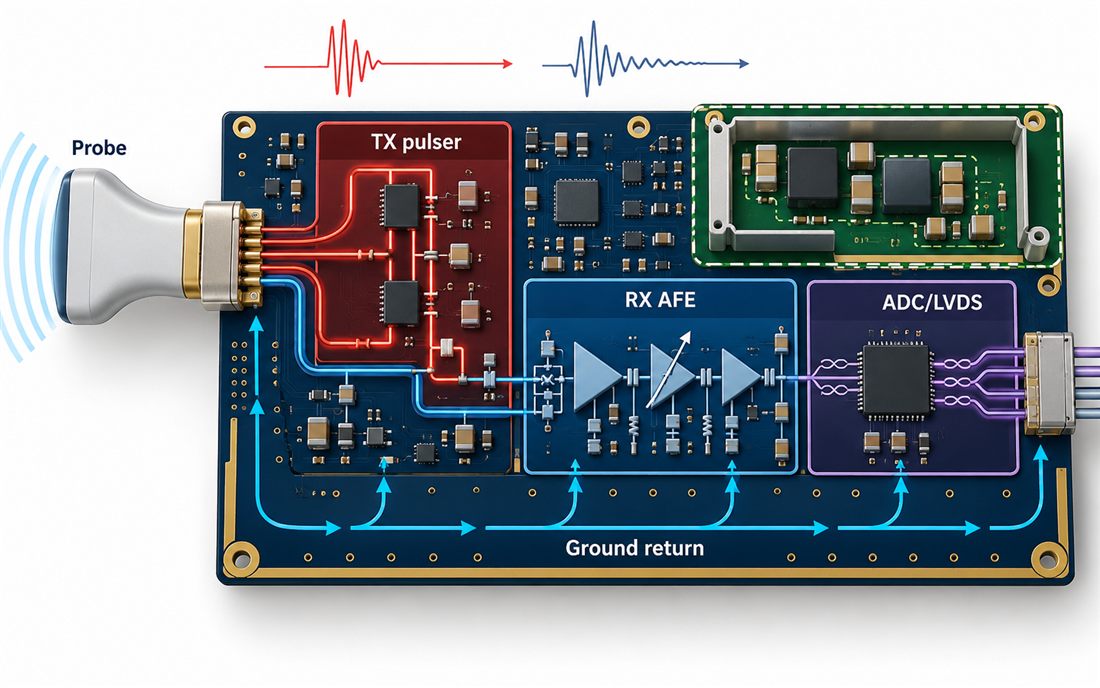
Conceptual layout showing physical separation of the probe, transmit pulser, receive AFE, ADC/LVDS and ground-return regions.
Control supply noise before it reaches the receive gain stages
High channel-count ultrasound boards combine pulser energy, low-noise amplification, programmable gain, ADC conversion, clocks, and digital links. TI’s AFE5807 guidance calls for low-inductance supply and ground connections, careful analog/digital interaction control, and symmetric differential routing. Place the local decoupling network at the device pins, but also define where the regulator current returns. A PCB manufacturing drawing that only specifies copper weight is incomplete; it should show the intended plane pair, via strategy, critical keep-outs, and impedance notes.
Do not treat the LVDS link as an afterthought. Keep each pair over a continuous reference, avoid stubs at the connector escape, and keep pair-to-pair skew inside the receiver guidance. For the AFE5807, TI gives a practical length-variation recommendation of less than 150 mil (3.81 mm) for related differential paths. The exact limit remains device- and interface-specific, so the release package should name the selected device and the rule used. A PCB assembly review should also check whether connector insertion, shielding hardware, and rework access can disturb those paths.
Separate the electrical noise problem from the thermal problem
AFE power regulators, pulser switches, ADCs, and clock devices do not dissipate heat in the same way. If a hot regulator is placed beside the receive input, thermal drift can appear as a gain or offset change even when the schematic is correct. Use copper spreading on the power side, but keep that copper from forcing a noisy return through the input reference. A industrial PCB assembly release should specify thermal pads, voiding expectations, and the inspection access needed to verify the power devices.
Turn the stack-up into a manufacturable signal-chain contract
For an ultrasound PCB, stack-up notes must become a supplier-readable manufacturing contract. Ultrasound boards often move between prototype and production suppliers. A stack-up that exists only in a CAD note will be reinterpreted. State dielectric thickness targets, copper layers, controlled-impedance nets, drill families, back-drill or via restrictions, and the plane that carries each critical return. When the design needs dense connector escape, HDI PCB manufacturing can be considered, but only when the via geometry and sequential build are agreed before routing. Otherwise, a conventional standard PCB build may be easier to control.
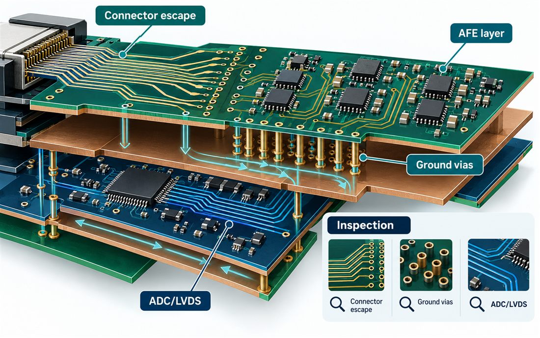
Conceptual cross-section highlighting connector escape, AFE layer, ground vias, ADC/LVDS routing, and inspection points.
At fabrication release, the PCB fabrication package should include the approved stack-up, impedance table, drill chart, copper balance instruction, and a marked-up drawing for the probe and shield interfaces. At assembly release, the SMT assembly package should identify moisture-sensitive parts, thermal profiles, connector coplanarity requirements, and the order in which shields or acoustic-interface hardware are installed.
Build a verification plan that catches noise before imaging trials
The ultrasound PCB should be verified with transmit and receive activity present, not only with a quiet receive test. A project team can reduce late surprises on an Ultrasound PCB by verifying the board in layers. First inspect the fabricated coupons and critical connector features. Then verify power-rail ripple and clock cleanliness with the board in a representative mechanical enclosure. Next exercise transmit and receive timing together, because a receive-only check can miss coupling from the pulser. Finally compare channels across gain settings and cable configurations. These are engineering checks and design targets, not claims of a particular customer measurement.
- Confirm that the probe connector datum and shield return match the drawing.
- Check every sensitive trace for an uninterrupted reference and a nearby return-via option.
- Confirm differential pair length and impedance rules at the released revision.
- Review regulator placement, decoupling, thermal copper, and rework access.
- Record stack-up, drill, assembly, and change-control evidence with the build.
For a prototype-to-volume handoff, an Ultrasound PCB project should have its PCB design owner sign the return-path review, while the PCB fabrication owner signs stack-up and impedance feasibility. A PCBA owner then closes the assembly and inspection risks. This division prevents a project manager from discovering at pilot build that an electrical assumption was never converted into a production control.
Release decision
A stable ultrasound PCB is the result of controlled interfaces rather than a single component choice. The right Ultrasound PCB is not the board with the most copper or the shortest schematic. It is the board whose probe boundary, return system, supply network, multilayer geometry, and assembly method can all be explained and repeated. Before release, ask whether the receive path remains physically protected during transmit, whether the reference plane is continuous, whether the LVDS and clock rules are documented, and whether the supplier can inspect the features that matter. If any answer is vague, the design is not ready for a stable imaging trial.
Technical basis: Analog Devices ultrasound front-end guidance; Analog Devices MAX14808 PCB layout note; Texas Instruments AFE5807 data sheet and ultrasound reference-design material. Values quoted above are device guidance or engineering targets and must be reconciled with the selected AFE, probe, stack-up, and released fabrication drawing.
