HomeAuthor

kkpcb02 - KKPCB - Page 4 of 15

TLY-5 PCB RF Test Fixtures: A Reliable Calibration and Connector Interface Workflow

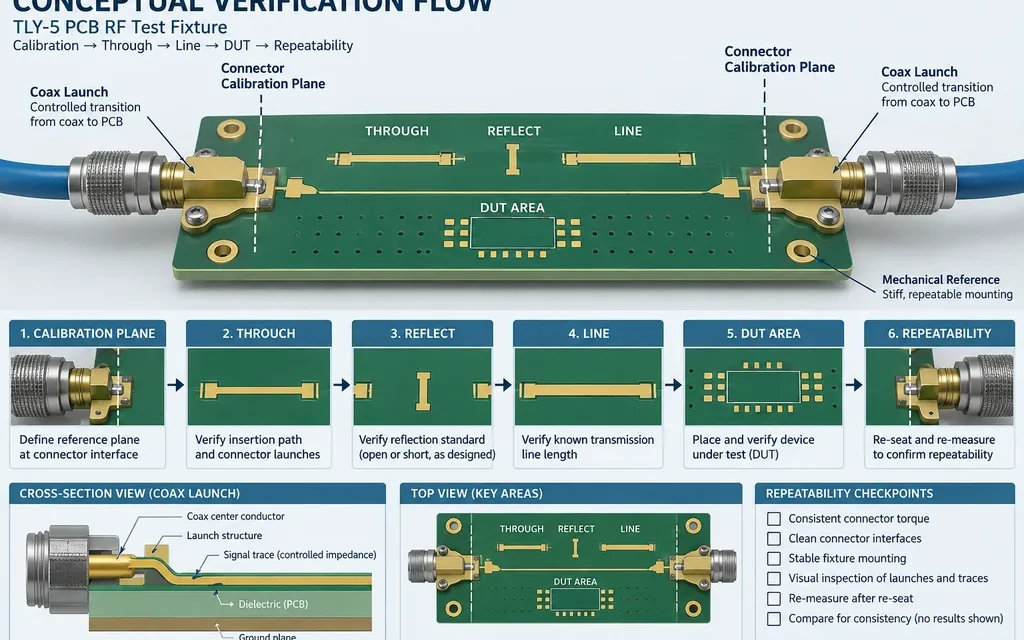
TLY-5 PCB RF test fixture design is often the hidden variable in a prototype program. A device under test can appear to have excess loss or phase drift when the real variation comes from connector wear, launch geometry, cable movement, or an undefined calibration plane. The fixture must be treated as an RF product with...
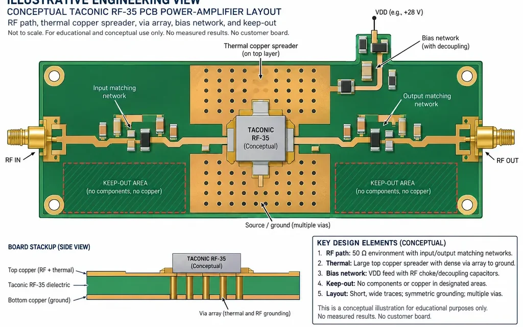
Taconic RF-35 PCB Power Amplifier Layout: A Robust Heat-Spreading Path That Protects RF Tuning

Taconic RF-35 PCB power amplifier thermal work must preserve two things at once: the device must shed heat, and the RF path must keep its intended impedance and return current. The common project failure is a late copper pour or thermal-via change that improves a temperature estimate but shifts the launch, bias isolation, or local...

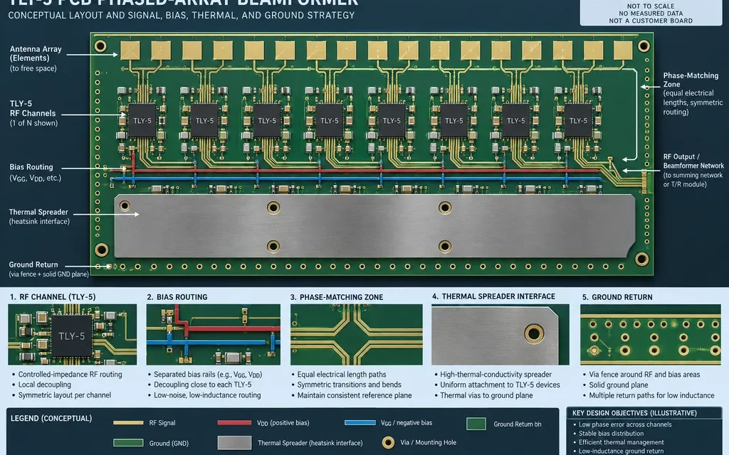
TLY-5 PCB in Phased-Array Beamformers: A Thermal and Bias-Routing Strategy

TLY-5 PCB beamformer thermal design is a coupled RF and power problem. In a phased array, each channel must preserve phase while bias networks, power amplifiers, control lines, and heat paths share a compact multilayer board. The engineering risk is not simply a hot spot; it is a hot spot that changes dielectric geometry, connector...

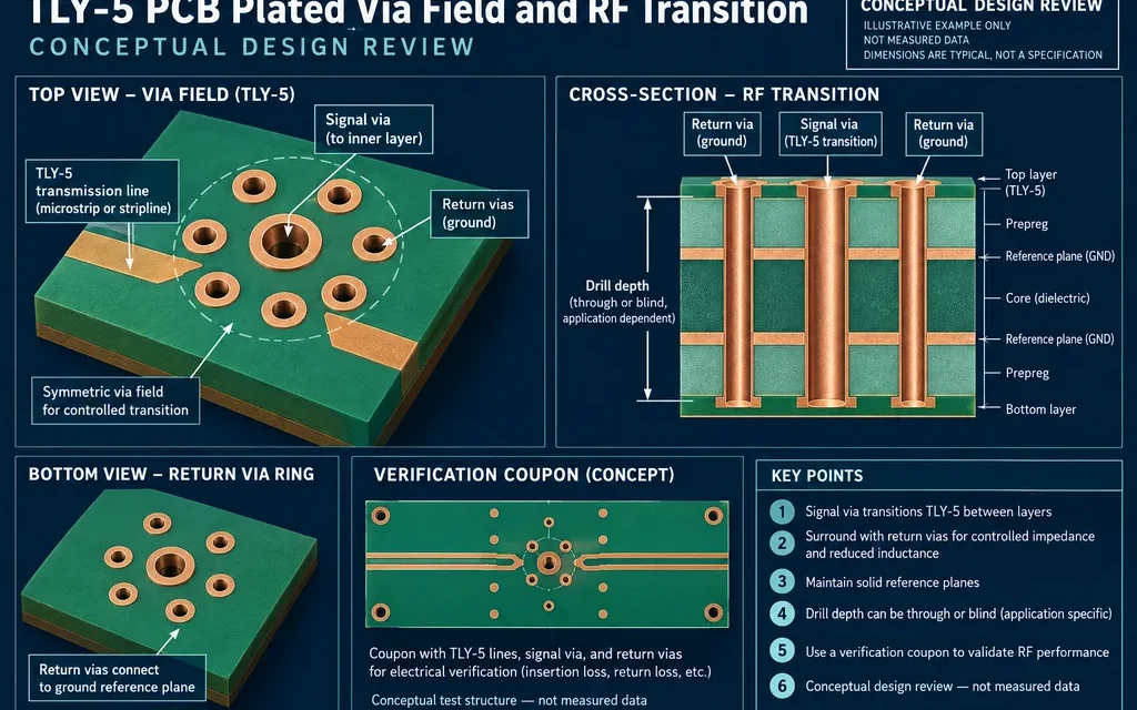
TLY-5 PCB Via Fields: Designing Plated Transitions Without Tuning Away the Real Problem

A TLY-5 PCB via field is not a cosmetic layout detail in a Ku-band module. The plated transition decides where the return current closes, how much barrel remains beyond the active layer, and whether the connector launch modeled by the RF team still represents the finished board. When this is released late, the first prototype...

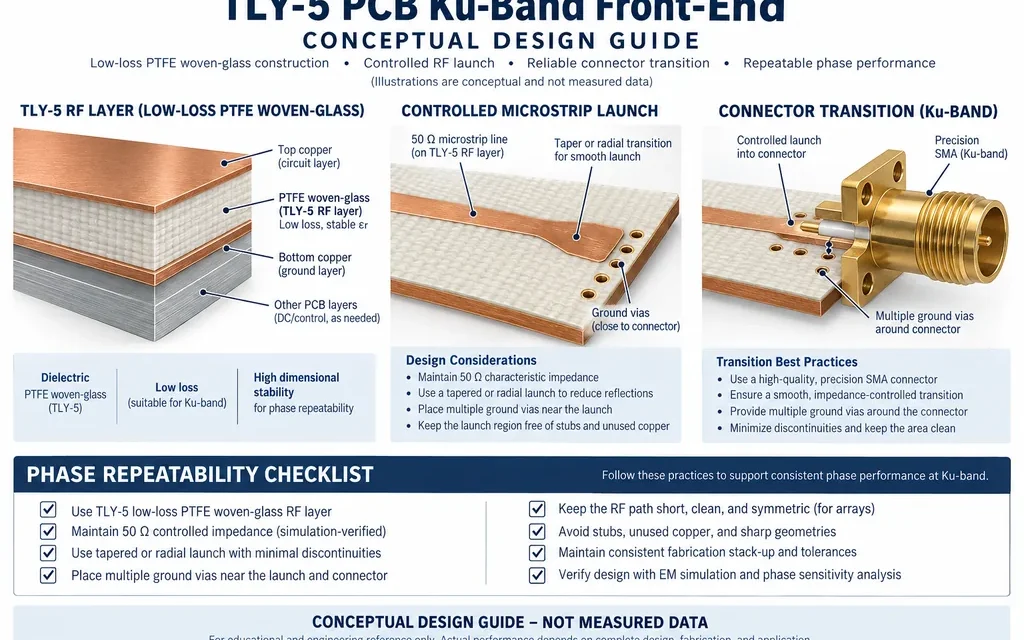
TLY-5 PCB for Ku-Band Front Ends: Managing Copper Roughness and Phase Repeatability

Ku-band TLY-5 PCB projects need a finished-board reference, not only a laminate name. Table of Contents Finished-board sensitivity Copper roughness Connector launch Phase repeatability Manufacturing handoff Release checklist TLY-5 PCB is often selected for a Ku-band front end because the laminate combines a low nominal dielectric constant with low dielectric loss. The difficult part is...

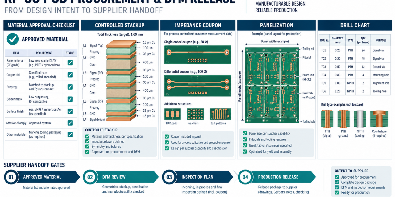
RF-35 PCB Procurement and DFM: A Supplier-Ready Release Checklist

Procurement teams often receive a microwave PCB package that looks complete but leaves the fabricator to guess the laminate grade, pressed dielectric, coupon method, or drill sequence. This supplier-ready checklist uses an RF-35 PCB example to turn design intent into controlled purchasing and DFM inputs without inventing customer results. RF-35 ceramic-filled PTFE/glass laminates are commonly...

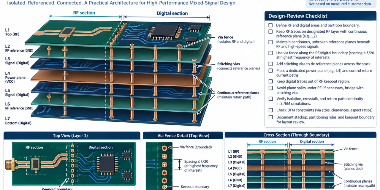
RF-35 PCB Mixed-Signal Stackup: Partitioning RF and Digital Return Paths

Mixed RF-and-digital boards rarely fail because the engineer forgot a trace-width rule. They fail when the stackup, plane strategy, and return path are treated as separate documents. This article uses an RF-35 PCB example to explain how a project team can partition RF and digital functions while keeping the board manufacturable. RF-35 ceramic-filled PTFE/glass materials...

RF-35 PCB Connector Launch and Via Transition: A Practical Verification Workflow

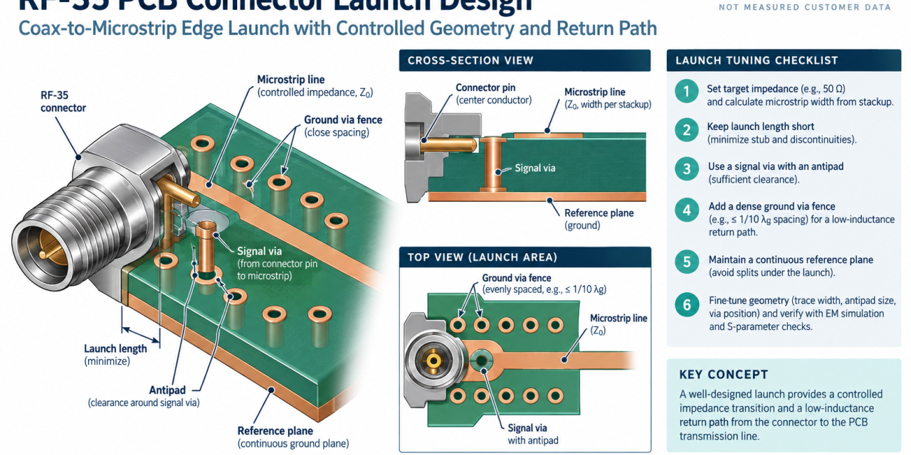
A connector launch is the shortest and most fragile transmission-line section on many microwave boards. The signal leaves a coaxial pin, crosses a pad and via, and then enters a controlled planar line. This guide uses an RF-35 PCB example to show how to release that transition with a defined return path, manufacturable clearances, and...

RF-35 PCB Thermal Stability: Controlling CTE, Registration, and Drill Reliability

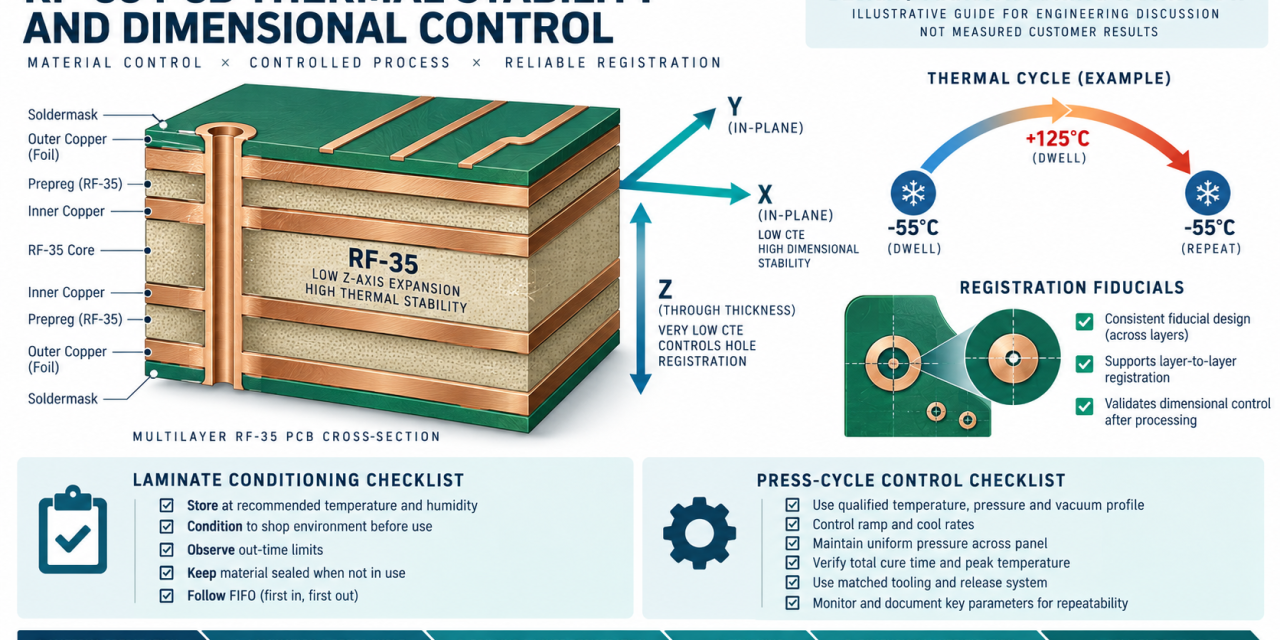
Thermal drift is an electrical problem when a microwave board moves enough to change trace geometry, connector alignment, or plated-hole stress. This article treats RF-35 PCB as a production material choice and focuses on the thermal-mechanical controls that keep a high-frequency design repeatable from panel build through assembly. Taconic RF-35 typical property tables report a...

RF-35 PCB Stackup and Controlled-Impedance Release for High-Frequency Designs

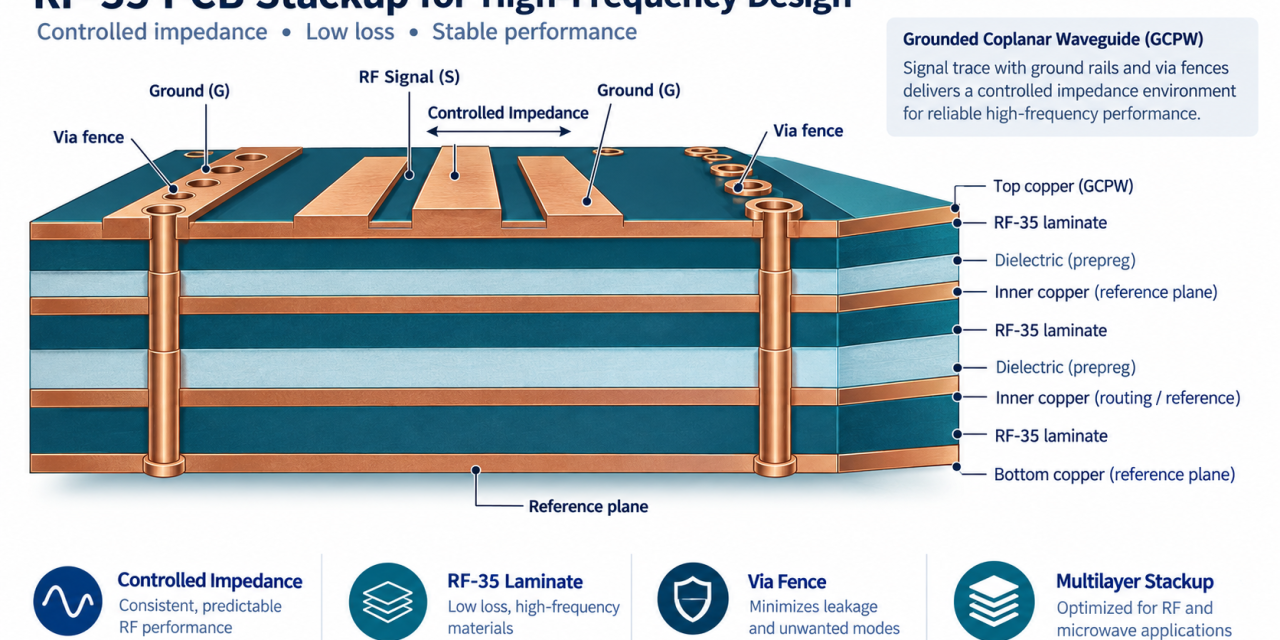
High-frequency board projects often fail at the handoff between an electrical stackup and a buildable panel. A designer may select a low-loss laminate, but the fabricator still needs a controlled dielectric thickness, a stable reference plane, and a practical drill-and-plate sequence. This guide uses an RF-35 PCB design example to show how to convert an...