HomeAuthor

kkpcb02 - KKPCB

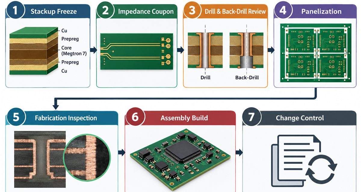
Megtron 7 PCB DFM Release: Panelization, Coupons, and ECO Control Before Volume Build

The most expensive Megtron 7 PCB problem is often a release problem, not a material problem. A prototype may route correctly, yet the volume panel has no representative coupon, uneven copper, an impractical depanelization rail, or an ECO that quietly changes the impedance construction. A useful DFM gate turns the electrical intent into a package...
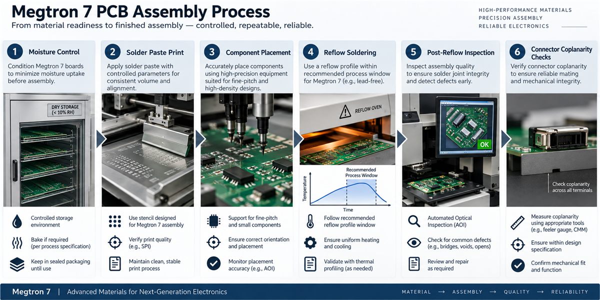
Megtron 7 PCB Assembly: Moisture, Reflow, and Coplanarity Controls for High-Speed Modules

A high-speed board can pass fabrication inspection and still lose performance during assembly. Moisture exposure, an unsuitable reflow window, connector coplanarity, or residue under a shield can change the mechanical position of a launch and weaken a controlled return path. A production-ready Megtron 7 PCB connects material handling to RF and signal-integrity requirements. Table of...

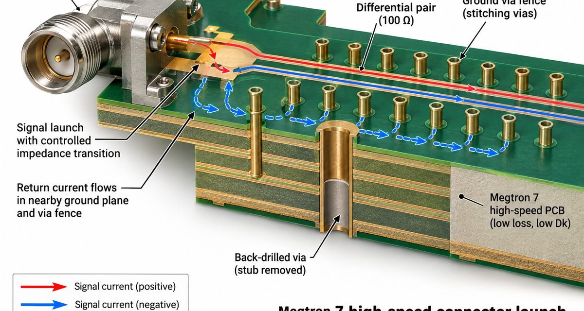
Megtron 7 PCB Connector Launches: A Back-Drill and Ground-Return Review for Multi-Gigabit Ports

Connector launches often become the hidden bottleneck in a high-speed program. The laminate may have a low loss tangent, but an unused barrel stub, a broken reference plane, or an asymmetric ground-via pattern can dominate the transition. Treat every Megtron 7 PCB as a small RF structure with its own geometry, datum, and verification plan....

How to Freeze a Megtron 7 PCB Stackup When Layer Count and Impedance Must Move Together

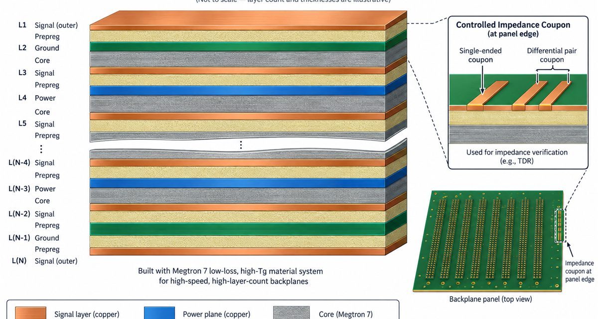
A Megtron 7 PCB stackup must be frozen as an electrical and manufacturing contract before layer count or impedance changes are approved. High-layer-count digital boards rarely fail because an engineer forgot to draw a trace. They fail when a late layer move changes dielectric thickness, resin distribution, or reference-plane continuity and the impedance model is...

Megtron 7 PCB Copper Profile and Glass-Weave Control for Long Backplane Channels

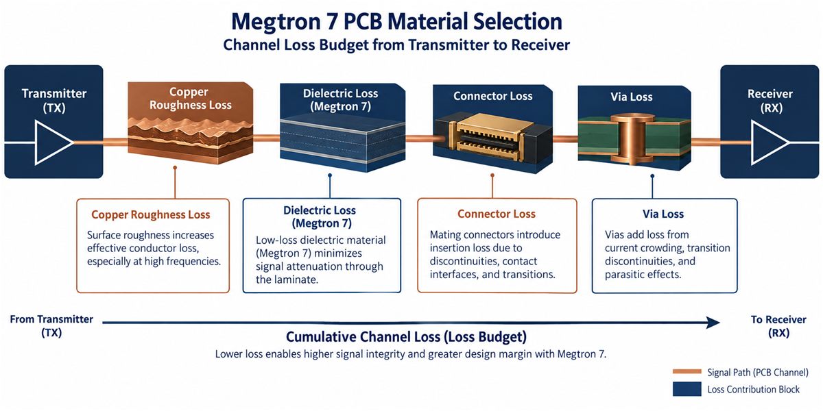
A long backplane channel can fail a design review even when the laminate choice looks correct on paper. The usual problem is not one dramatic defect; it is the accumulation of copper profile loss, dielectric loss, connector discontinuity, via loss, and local glass-weave skew. A useful Megtron 7 PCB project therefore starts with a channel...

Megtron 6 PCB DFM Release: The Production Checks That Protect High-Speed Yield

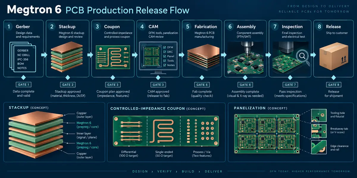
The released Megtron 6 PCB construction is the reference for the DFM package. Any supplier change to a Megtron 6 PCB must carry the same stackup and coupon revision, so procurement can compare capacity without changing electrical intent. Megtron 6 PCB DFM release work is where a high-speed design becomes a repeatable production definition. A...

Megtron 6 PCB Assembly: A Reflow and Connector-Launch Plan for High-Speed Modules

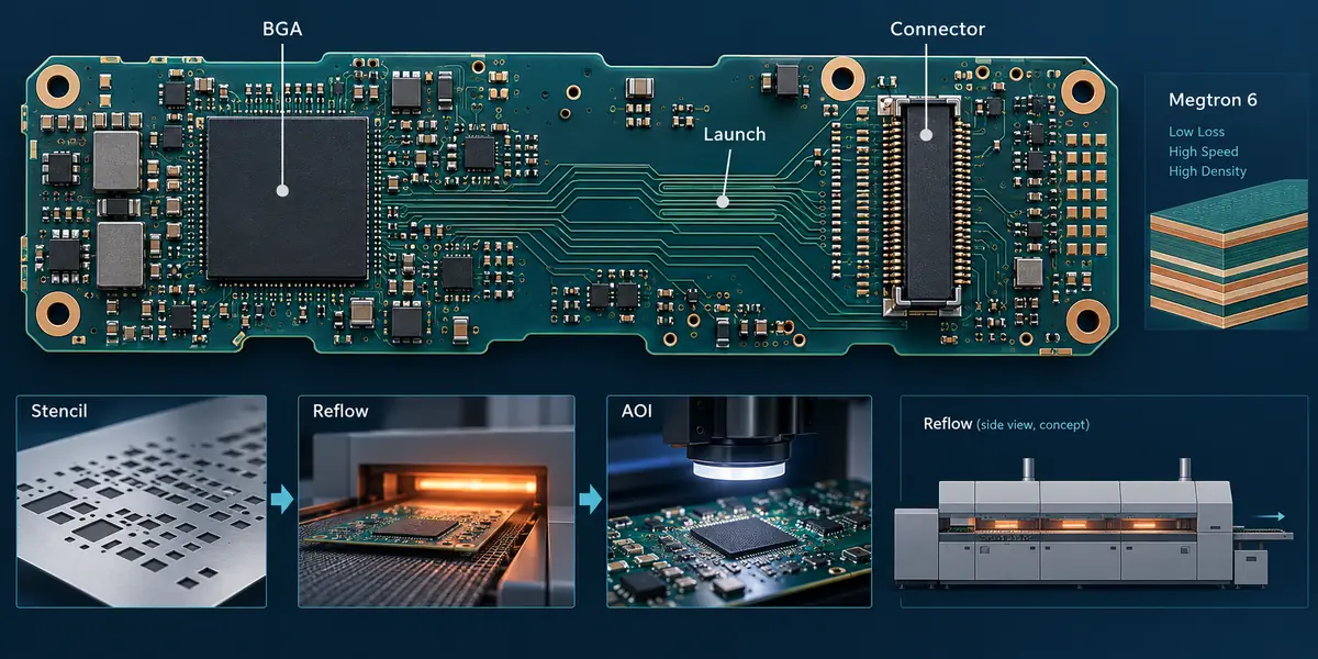
The Megtron 6 PCB connector launch remains the shared datum for SI and assembly inspection. The production Megtron 6 PCB callout should travel with the reflow and inspection package. A connector change on a Megtron 6 PCB is an electrical and assembly change, not only a mechanical edit. For the release team, a Megtron 6...

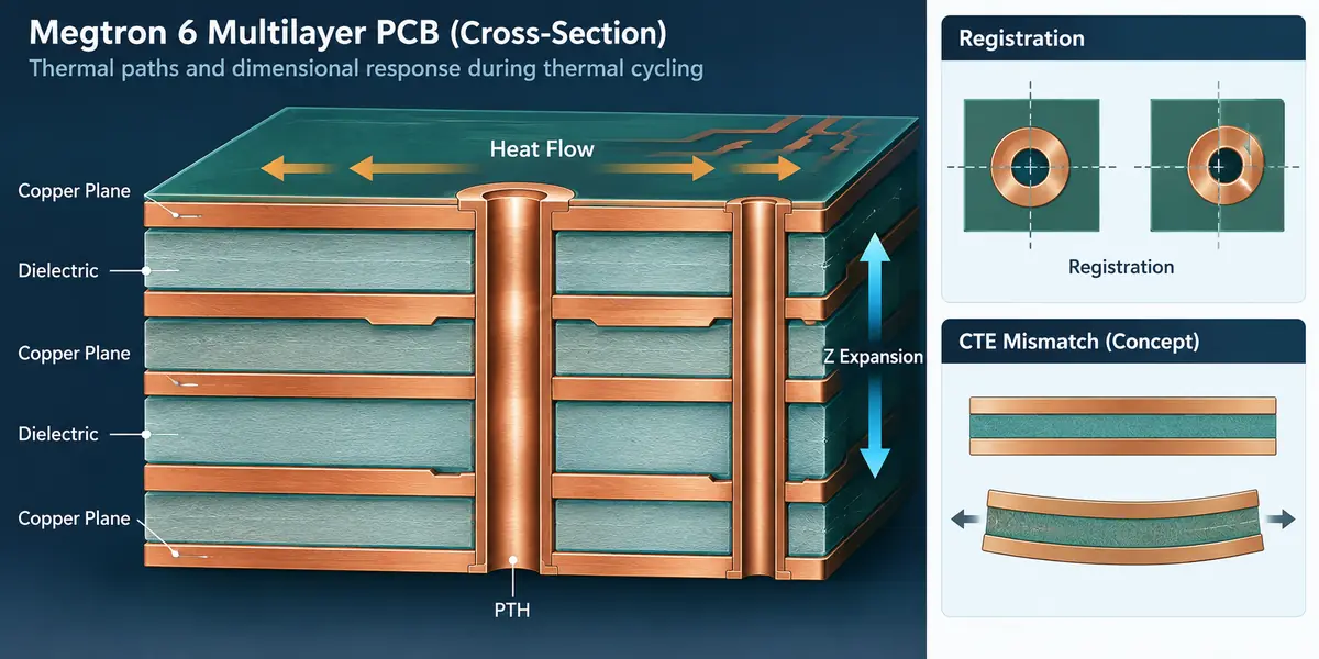
Megtron 6 PCB Thermal Cycling: Keeping Dense Multilayer Registration Predictable

The controlled Megtron 6 PCB datum should be reviewed before thermal cycling begins. For a dense compute Megtron 6 PCB, copper balance and registration targets belong in the same release package. A second Megtron 6 PCB construction should never be approved without a revised coupon plan. Megtron 6 PCB thermal reliability is a registration problem...

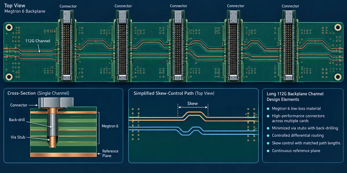
Megtron 6 PCB for 112G Backplanes: Managing Skew, Vias, and Reference-Plane Continuity

Table of Contents Channel construction Skew and weave control Via and plane continuity Coupon and release checks The released Megtron 6 PCB stackup must keep the 112G lane assumptions visible to design and fabrication. At this data rate, a small skew shift, a poorly referenced via field, or a connector launch that changes between panels...

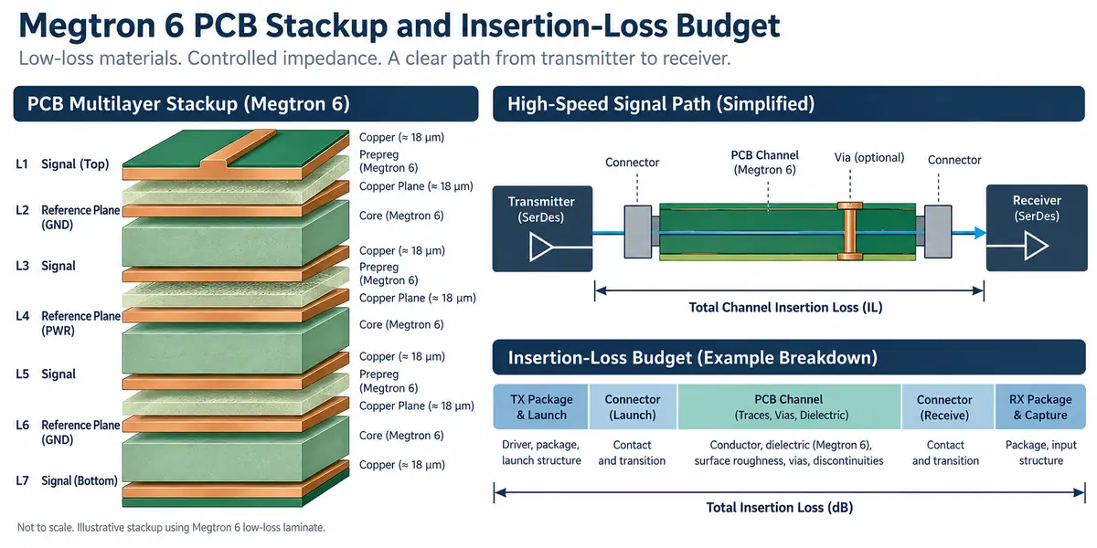
Megtron 6 PCB Material Selection: Turning Loss Budgets into a Manufacturable Stackup

Megtron 6 PCB projects often fail late for a simple reason: the electrical loss budget was written before the stackup, copper profile, and connector geometry were frozen. A material family can support demanding high-speed channels, but the released board still depends on resin content, finished dielectric thickness, reference-plane continuity, copper roughness, and fabrication capability. This...