
A launch environment turns a seemingly rigid electronics box into a coupled mechanical system. The spacecraft structure, chassis, mounting hardware, board, connectors, cable harness, and component masses all exchange load. If a Satellite PCB is treated as a bare laminate rather than a mounted assembly, the first resonance or a heavy connector can concentrate strain at solder joints, vias, or a board edge. A successful design review begins by asking where the assembly is supported, how loads enter it, and which interfaces the project will actually qualify.
Trace the mechanical load path
For a Satellite PCB flight assembly, start with the launch vehicle or platform environment supplied by the responsible systems team, then follow the load through the spacecraft panel, chassis, standoffs, board, component packages, connector, and harness restraint. Do not translate a generic acceleration value into a board-level claim without the boundary conditions, axis, frequency content, damping, mass distribution, and test configuration. NASA’s historical printed-circuit-board vibration guidance discusses board flexure near resonance and the influence of support and damping; it should be read as design context, not as a current qualification limit for a specific mission.
For a Satellite PCB, create a simple interface map before the layout is frozen: board outline and thickness, support locations, fastener type, component mass and center of gravity, connector mating direction, harness route, and enclosure clearance. The mechanical and electrical teams should share a coordinate system and controlled drawing revision. This gives each Satellite PCB mounting feature a common inspection datum. A PCB layout review can then identify where copper, vias, slots, keep-outs, and large packages interact with predicted flexure rather than reviewing the two disciplines in isolation.
Support the board where it matters
A Satellite PCB support strategy is not simply a matter of adding screws. Closely spaced supports may improve local stiffness but increase assembly complexity, create tolerance stack-up, or interfere with high-voltage clearance and thermal interfaces. A long unsupported span can place components or connectors at a high-deflection region. The right pattern depends on the board geometry, enclosure stiffness, mass loading, and specified dynamic environment. Use the structural model to identify likely high-response zones, then make the board support, stiffener, or damping choice with the mechanical authority. Review the Satellite PCB design again if the enclosure stiffness or support boundary changes.
Keep heavy or tall components near adequately supported regions when the electrical architecture permits. Where a component must sit on a flexible span, review its package, pad geometry, lead or termination style, local copper balance, and inspection access. Avoid abrupt routing and copper-density changes that coincide with a mechanically sensitive neck. Any stiffener or support feature must be reflected in the released stackup and fabrication drawing; a late mechanical addition can alter board flatness, local heat flow, connector fit, and rework access.
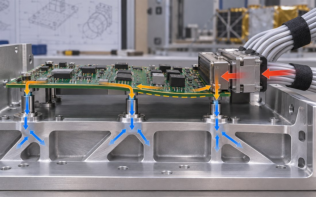
Coordinate these decisions with the rigid-flex PCB or rigid-board construction, as applicable. A flex region changes how mechanical strain is distributed; bend radius, copper layer position, coverlay opening, adhesive system, and transition location are all relevant. A rigid-flex assembly also needs a defined handling and fixture plan so that the flexible section is not used as an unintended lifting or clamping point.
Protect connector and harness interfaces
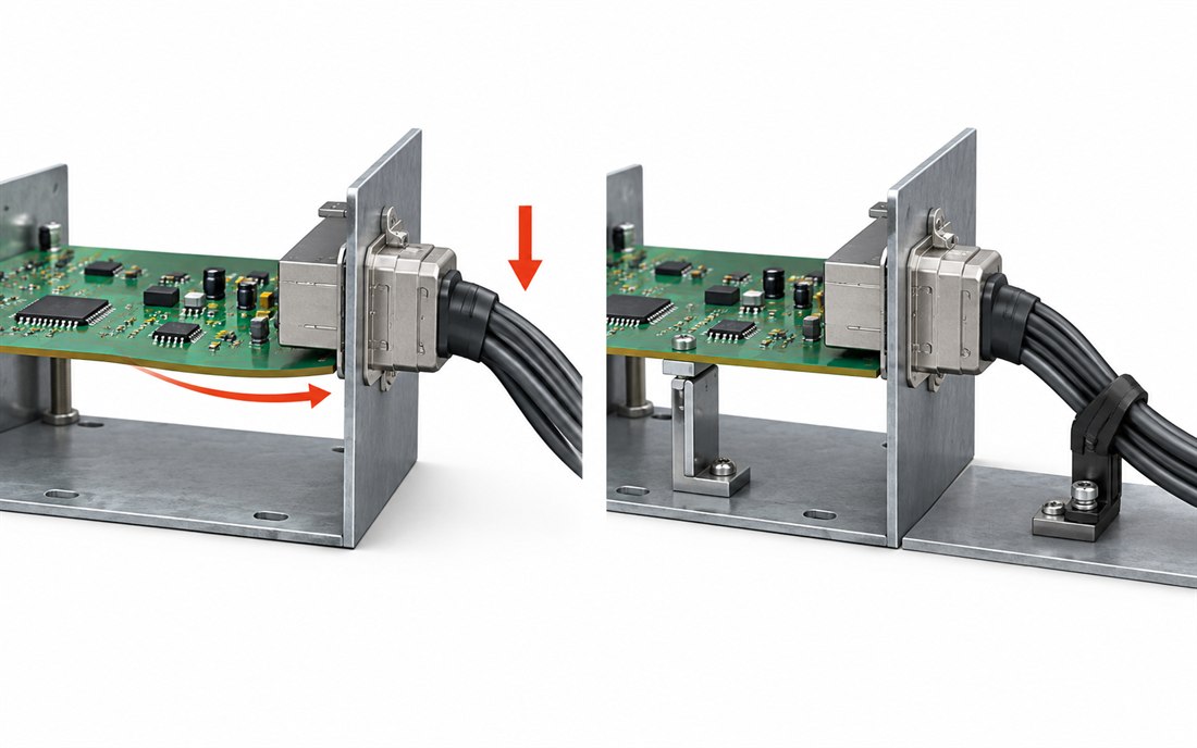
Connectors often create a local mechanical problem even when the main board span is acceptable. A board-edge RF connector, a cable with substantial stiffness, or repeated mating can apply bending moment to solder joints and nearby laminate. Define which part carries the load: the connector shell, bracket, chassis, board, or a separate strain-relief feature. Ensure that the mating-force direction, screw access, cable bend radius, and keep-out zone match the actual assembly sequence.
For a Satellite PCB RF interface, the connector body and soldered signal pin should not be assumed to provide structural restraint. Transfer cable and mating loads into the chassis or a dedicated support when the system design calls for it. For a Satellite PCB, keep the RF launch, ground tabs, chassis bond, and support features within one mechanical-electrical definition. PCB assembly instructions should specify connector alignment, soldering method, inspection views, and any post-assembly fastening step.
Harness restraint must prevent cable mass from repeatedly loading the board while leaving adequate service slack and respecting shielding continuity. The through-hole connector process may offer a different mechanical interface from a surface-mount connector, but neither is automatically robust without an agreed load path. Inspect the solder fillet, barrel or pad, nearby laminate, and hardware after the specified test sequence. Record any repair and do not treat an unplanned rework as equivalent to the released build.
Plan modal and vibration evidence
Analysis is useful when its boundary conditions are realistic and its correlation plan is clear. Capture the Satellite PCB and enclosure mass properties, fastener and contact assumptions, material and thickness inputs, damping assumptions, and the location of the applied excitation. A modal survey can help locate resonances; a sine or random vibration sequence must be selected by the responsible mission authority. Do not use a published historical test level as a substitute for the current project specification.
Define inspection before and after test: visual examination, electrical continuity, connector retention, board-to-chassis clearance, and any component-specific checks. Where the board carries RF or precision analog functions, record the measurement baseline and repeat the same calibrated measurement after vibration. Separate pass/fail limits from data collected for engineering correlation. A prototype build is valuable only when its mounting, cable restraint, mass loading, and connector hardware represent the intended flight configuration.
Production quality depends on the released package as much as the test. Tie the board outline, drilled holes, stackup, material, copper balance, connector footprint, assembly drawing, and inspection criteria to the same revision. Confirm the RF material selection and SMT assembly route against that baseline. A multilayer PCB build may satisfy its electrical construction while still requiring a separate mechanical review of support spans and component placement. For a manufacturing release, identify controlled dimensions, edge treatment, hole tolerances, and any local stiffening requirements explicitly.
Release a controlled mechanical baseline
Before procurement, the project manager should confirm that the approved mechanical model, native board data, fabrication drawing, assembly drawing, BOM, connector specification, and test plan refer to one baseline. Open questions need an owner and due date: who approves a support change, who controls a connector alternate, who evaluates a mass-property change, and who determines whether a repair requires retest? This avoids a common schedule failure in which a supplier receives a new enclosure or connector detail after the board has already been released.
- Obtain the current mission dynamic environment and the exact test configuration from the responsible design authority.
- Map board supports, component masses, connector loads, harness restraint, and chassis interfaces.
- Review high-response areas against component placement, copper changes, slots, vias, and flex transitions.
- Specify connector load relief, inspection access, handling limits, and post-test checks.
- Correlate the analysis to representative hardware and keep test data distinct from design assumptions.
- Control every drawing, stackup, BOM, and assembly change through a documented impact review.
For engineering teams, the most useful release is one that makes the physical load path inspectable and the change boundary explicit. A Satellite PCB is not qualified merely because a bare board survived an undefined bench test; the assembly, support, connector, and harness configuration must match the requirement. State what was analyzed, what was measured, and what remains an assumption.
Sources: NASA NTRS, “Guidelines for Vibration Life Extension of Printed Circuit Board Assemblies” (historical design guidance); NASA NTRS, “Lumped Parameter Modeling for Rapid Vibration Response Prototyping and Test Correlation for Electronic Units.” These references support general vibration-design and correlation principles; they do not define a KKPCB test result or mission qualification.





