
A Satellite PCB can pass electrical inspection on the bench and still become a contamination source after launch. In vacuum, volatile compounds have no convective path away from the assembly; they migrate and may condense on colder optical, RF, thermal-control, or detector surfaces. The engineering question is therefore not simply whether a laminate has a favorable data-sheet value. The team must connect material selection, process residues, component packages, cleaning, bakeout, and mission-specific contamination limits to one controlled release decision.
For a program manager, the late failure mode is often a missing evidence chain: the board supplier has a material declaration, assembly has a cleaning record, and the payload team has a contamination budget, but nobody has shown that the complete configuration meets the project’s acceptance basis. A spacecraft assembly integration work package should define these interfaces before the first engineering unit is built.
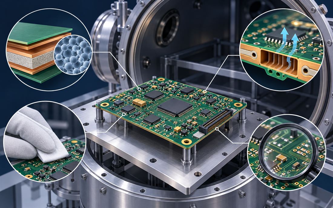
For Satellite PCB Vacuum Design, Map the Exposed Surfaces
For a Satellite PCB program, build a contamination map of the assembled payload. Identify optical apertures, cold radiators, antenna or filter surfaces, high-impedance nodes, moving mechanisms, and enclosed cavities. For each sensitive surface, record its temperature range, line of sight to the board, allowable deposition or performance shift, and whether a shield or cover changes the transport path. This makes “low outgassing” a system requirement that can be evaluated rather than a vague purchasing preference.
In Satellite PCB material review, decompose the board into what is actually exposed: laminate and resin edges, solder mask, legend ink, surface finish, conformal coating if permitted, adhesives, underfill, cable materials, connector inserts, and component encapsulants. A board-level material choice is only one part of the inventory. The Satellite PCB placement review should also show which materials face the cold or optically sensitive surfaces and whether the assembly has blind pockets that retain cleaning chemistry.
Satellite PCB Material Approval: Use ASTM E595 Within Its Limits
NASA’s outgassing program describes the ASTM E595 screening method using total mass loss (TML) and collected volatile condensable material (CVCM). Such results are useful for comparing candidate materials under a defined laboratory procedure; they do not prove that a populated PCB, a specific adhesive stack, or the complete flight assembly is acceptable. For a Satellite PCB, data must be tied to the exact product, cure state, lot or formulation, thickness, and test record. If those details differ from the production configuration, record the gap rather than treating a database hit as a blanket approval.
A common project trap is to transfer an acceptance threshold from a different customer or mission. Use the program’s applicable material-control plan and contamination budget. If a source gives a typical test result, describe it as a material screening value—not a board qualification. The Satellite PCB engineering package should identify who approves substitutions, what evidence accompanies them, and how change control is handled after qualification.
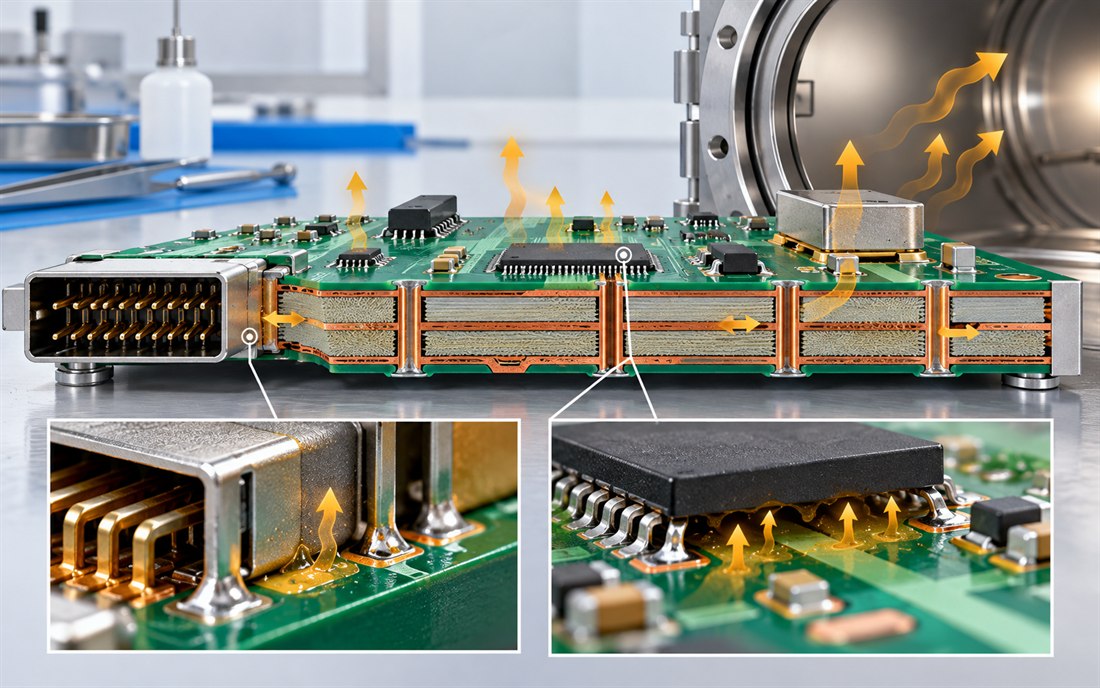
Satellite PCB Assembly: Control Residues and Hidden Reservoirs
Outgassing and contamination are not interchangeable. A residue may be nonvolatile at room temperature yet become mobile during a thermal cycle; a material may have acceptable screening data but be assembled with flux, handling films, protective coatings, or cleaning residues that were never included in the evidence set. For Satellite PCB assembly, specify the approved soldering chemistry, cleaning method, rinse quality where applicable, drying procedure, handling controls, and visual or ionic-cleanliness acceptance method in the build traveler. The Satellite PCB fabrication notes should call out resin-rich edges, cavities, via structures, and surface-finish interfaces that are difficult to clean or inspect.
For assembly, align the approved component list and package materials with the process. Plastic-packaged devices, connector inserts, labels, staking compounds, and local coatings may contribute more uncertainty than the bare board. Confirm whether any package or polymer absorbs the selected cleaning solvent, and avoid introducing a new bakeout temperature without checking component and assembly limits. A NASA smallsat knowledge-base note warns that bakeout conditions are provider- and hardware-specific; a temperature that helps one material can damage another component or drive contaminants toward a sensitive surface.
Satellite PCB Bakeout Must Be a Controlled Process
For Satellite PCB bakeout, define the purpose, starting cleanliness state, temperature profile, pressure or purge environment, duration, thermal uniformity, fixture materials, witness samples if required, and post-process packaging. The exact profile belongs to the mission’s approved process plan; do not infer one from a generic web value. Consider whether the board is bare, partially assembled, or fully populated. These states have different thermal mass, volatile inventory, shadowing, and component constraints.
Use a documented change-impact review when laminate, solder mask, finish, flux, cleaning agent, adhesive, or component package changes. The review should answer whether new outgassing data or a repeat cleanliness assessment is required, whether thermal-vacuum screening is affected, and who accepts the residual risk. The Satellite PCB release should preserve the approved bill of materials and process revision, not merely a purchase-order description.
Release Evidence for a Satellite PCB Flight Build
A practical Satellite PCB release package contains the exact material and process identifiers; available supplier declarations and test records; approved deviations; cleaning and bakeout records; inspection results; packaging and storage controls; and a traceable link to the mission acceptance criteria. Mark every value by evidence type: published typical data, program design limit, supplier test result, or measured result from the actual unit. Do not label an illustrative engineering example as a KKPCB customer qualification.
- Map contamination-sensitive surfaces and potential transport paths.
- Verify material data against the exact formulation and production condition.
- Include assembly polymers, fluxes, coatings, and connector materials in the review.
- Set cleaning, drying, handling, and bakeout controls with explicit owners.
- Reopen the assessment after a material, process, or configuration change.
For teams coordinating supply-chain evidence, PCB production planning can be tied to a controlled build package; prototype assembly is useful for evaluating process sequence before a formal qualification build; SMT assembly must preserve the approved thermal profile; through-hole assembly may introduce different flux and cleaning needs; and high-frequency PCB materials should be evaluated for the actual RF function as well as contamination constraints. For mechanical integration, compare rigid-flex PCB options only when the design requires them, and include HDI interconnect choices in the cleaning and inspection access review. Finally, use the documented RF design capability and assembly process review as supplier interfaces—not as substitutes for mission approval.
Sources: NASA Outgassing Database and ASTM E595 test description; NASA-STD-6016C with Change 1; NASA Small Spacecraft Systems Virtual Institute knowledge base, “Bake Out”; NASA workmanship guidance for printed circuit boards. These references support material-screening and process-control principles; project-specific acceptance criteria remain controlling.





