
Medical PCB layout for a low-level biopotential front end starts with a simple discipline: treat the sensor input, its reference, and its return path as one small system before placing anything noisy nearby. ECG, EMG, impedance, and other low-amplitude acquisition paths can be affected by switching current, digital edge energy, cable pickup, and unintended return loops. A layout cannot determine device compliance by itself, but it can make later verification clearer or unnecessarily difficult.
The useful question is not whether a board looks neatly divided into analog and digital zones. The useful question is whether every low-level signal has a deliberate path from connector to front end, a controlled reference, and a predictable path back. That review should begin before the placement becomes dense enough that a quiet route has to cross a power region or squeeze around a processor.
Begin with the sensor path and its return
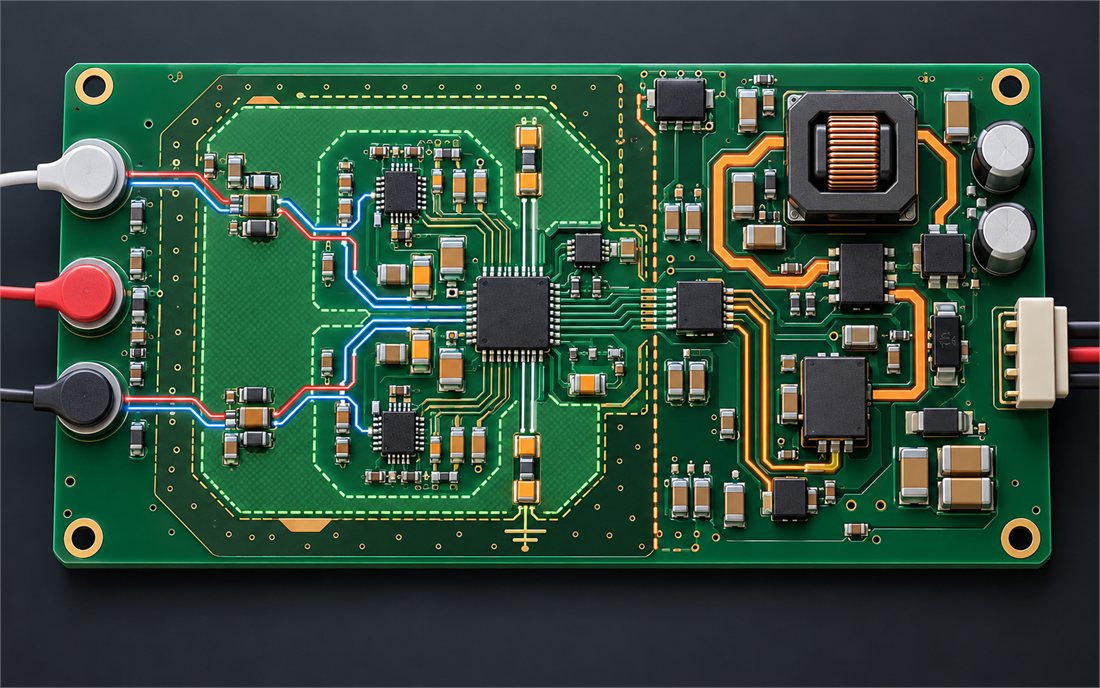
Place the input connector, protection network, bias components, analog front end, and first filtering stages so that the sensitive conductors are short and understandable. Route differential pairs as a pair where the circuit requires it, with comparable surroundings and without casually splitting their return environment. Keep test points, jumpers, and connector transitions out of the first few millimeters of a very low-level path unless they serve a documented purpose.
A solid reference plane is often more helpful than a decorative analog island. If a gap, slot, or mechanical keep-out forces a return current to detour, the route above it can behave differently from the intended schematic connection. Review connector shields, chassis features, and cable drains separately from the functional signal reference; combining them by habit creates ambiguity when noise troubleshooting begins.
Keep switching energy out by geometry
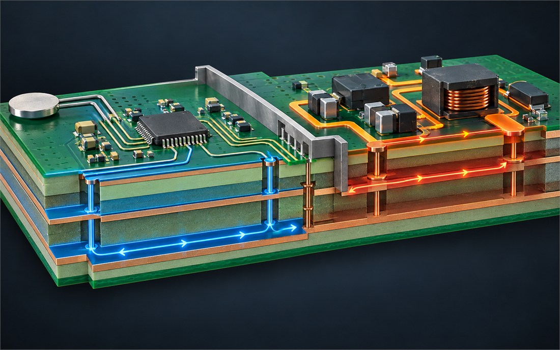
A converter is not only an electrical block. Its inductor, diode or synchronous switches, hot loop, input capacitors, output capacitors, and return copper form a high-energy physical region. Put that region away from the sensor connector and low-level amplifier inputs. Avoid routing sensitive traces underneath the inductor or through the converter’s return-current path. If a power stage must be on the same board, establish a boundary, then verify it on every copper layer rather than only on the top-layer placement view.
Digital interfaces need the same attention. Fast clocks, memory buses, display interfaces, and radio modules can couple energy through common impedance, reference discontinuities, or simple proximity. Separate the timing-critical digital area from the acquisition area, route each signal with an appropriate reference, and identify where the domains intentionally meet. A controlled meeting point is easier to review than a collection of accidental crossings.
Turn layout intent into a stackup decision
Layer assignment should help the physical partition survive routing pressure. Reserve nearby reference planes for sensitive signal layers, identify where power copper is allowed, and decide which vias can enter or leave the quiet region. A stackup review should also consider fabrication practicality: copper weights, drill structures, impedance needs, and what a fabricator must know to build the intended layer relationship. Do not wait until the data package is released to ask whether the plane strategy can be manufactured as drawn.
Use a review sequence that exposes conflicts
A compact cross-functional review is more effective than a late-stage visual inspection. First trace the input path from connector to amplifier. Next follow its return path and identify any gaps, vias, plane changes, or enclosure interfaces. Then inspect the power converter loop and fast digital routes on every layer. Finally, compare the result with the assembly plan: component orientation, cleaning access, shielding hardware, test access, and inspection needs can alter the practical layout.
Document the decisions that matter: sensitive keep-out boundaries, controlled return regions, grounding intent, and any exception that was accepted with a reason. That record helps a future revision distinguish intentional tradeoffs from mistakes introduced by a last-minute placement change.
Seven release rules for low-noise layouts
- Keep the sensor path, its protection, and its return physically understandable.
- Do not route a sensitive trace over a split, slot, or uncertain reference.
- Locate the converter hot loop away from the low-level input region.
- Review every layer, not only the top-layer placement view.
- Identify intentional domain crossings and their return path.
- Confirm stackup constraints with the fabricator before data release.
- Record every accepted exception so it can be reviewed on the next revision.
Source note: This is general layout-planning guidance. Device performance, risk controls, verification methods, and regulatory obligations remain the responsibility of the device manufacturer and its engineering team.
Related KKPCB capabilities
- Medical PCB planning for sensor, power, and mechanical interfaces.
- Medical PCB manufacturing review before a released data package.
- Medical PCB build discussions with fabrication and assembly inputs aligned.
- Medical PCB DFM communication for controlled production changes.
- Medical PCB projects that need documented handoff decisions.
- PCB Manufacturing options for stackup, materials, and fabrication data review.
- High Frequency PCB know-how when signal behavior must be considered early.
- HDI PCB approaches for dense interconnect and constrained routing.
- Multilayer PCB construction support for planned reference planes and routing layers.
- PCB Prototype builds for checking the released design before a larger run.
- Rigid-Flex PCB coordination where mechanical motion shapes the circuit.
- PCB Assembly review for process-sensitive component and cleaning choices.
- PCB Prototype Assembly support for early build learning.
- BGA PCB Assembly considerations for fine-pitch component placement and inspection planning.
- SMT PCB Assembly process input for repeatable component placement and reflow.
