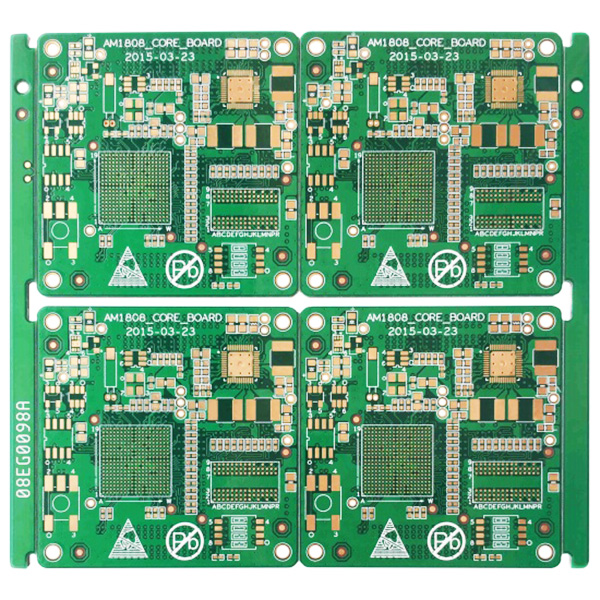
KKPCB provides end-to-end PCB solutions, from design support and rapid prototyping to mass production of HDI, rigid-flex, aluminum, and RF circuit boards. Serving global clients across telecommunications, automotive, industrial, medical, aerospace, and instrumentation sectors, we specialize in solving complex PCB challenges with advanced technologies such as HDI structures (1+N+1, 2+N+2, 3+N+3), embedded/blind vias, and multilayer designs. Utilizing high-TG materials and low Dk/Df dielectrics, we ensure superior performance and reliability. Our manufacturing adheres to IPC-6012 Class 3 standards and holds ISO 9001, IATF 16949, UL, and other international certifications, guaranteeing compliance with industry requirements.

HDI (High-Density Interconnect) PCB is an advanced printed circuit board technology that enables high-density circuit distribution using micro blind and buried via technology. HDI boards feature both internal and external circuits, connected through precise hole drilling and metallization processes to achieve reliable interlayer connections.
Typically manufactured using build-up technology, the technical complexity increases with the number of lamination layers. Standard HDI boards usually use a single buildup, while advanced HDI boards adopt secondary or multiple lamination techniques, combined with cutting-edge methods such as via stacking, plated hole filling, and laser direct drilling.
With ongoing technological development, electronic design continuously improves device performance while reducing size, meeting the demand for miniaturization across applications — from mobile phones to smart defense systems. HDI PCBs are essential in enabling compact, high-performance, and reliable electronic devices in today’s fast-evolving technology landscape.
High density interconnects (HDI) PCB is an indispensable part of the electronics industry. Electronic components become smaller and lighter, but performance needs to be improved. To accommodate this situation, you need to pack more features into a smaller area. This is what HDI PCB provides.
Compared with traditional PCB, HDI PCB has a higher unit circuit density. They use a combination of buried and blind holes, as well as microvia with a diameter of 0.006 inch or less.
The strict tolerances involved in using HDI printed circuit boards mean that you need to work with experienced suppliers. Even small defects or layout accidents can lead to serious problems. As a leading supplier of HDI printed circuit boards, KKPCB PCB provides a first-class circuit board, and its circuit density is much higher than that of traditional PCB.
At KKPCB, we provide advanced HDI PCB manufacturing solutions designed for high-speed, high-density, and high-reliability electronic applications, including AI computing systems, telecommunications, automotive electronics, industrial control, and RF/microwave systems.
Our HDI technologies support any-layer interconnection structures with stacked, staggered, and skip microvias, as well as copper-filled vias, via-in-pad plating, and advanced via fill processes to ensure excellent electrical performance and assembly reliability. We support complex HDI build-up designs from 1+N+1 up to 9+N+9, enabling ultra-high routing density for next-generation electronic systems.
Our manufacturing processes include sequential lamination, blind and buried vias, and Laser Direct Imaging (LDI) technology, ensuring high-precision alignment and stable multilayer registration. We are capable of producing ultra-fine circuitry down to 0.05 mm line/space and supporting fine-pitch BGA designs down to 0.3 mm.
To meet demanding signal integrity and RF performance requirements, KKPCB offers a comprehensive range of advanced materials, including low-loss laminates (I-Speed, FR408HR, Megtron 4, EM-888, N4000-13 series, TU-872 series), high-speed digital materials (Megtron 6, I-Tera MT40, Tachyon 100G, TU-883, IT-968 series), and RF/microwave laminates (Rogers RO4000/RO3000 series, RT/Duroid 5880, Taconic TLY series, Astra MT77). These material systems enable superior impedance control, low signal loss, and excellent thermal and electrical performance for high-frequency and high-speed applications.
| Description | Standard | Advanced |
|---|---|---|
| Line / Space | 45 / 50 μm | 35 / 40 μm |
| Laser Microvia / Pad | 75 / 200 μm | 50 / 150 μm |
| Mechanical Via / Pad | 150 / 300 μm | 125 / 250 μm |
| Thinnest Core Material | 50 μm | 50 μm |
| Thinnest Dielectric | 60 μm | 50 μm |
| Conductor Width Tolerance | ±20% | ±15% |
| Solder Mask Alignment | ±25 μm | ±15 μm |
| Layer Count | Up to 58L | Up to 68L |
KKPCB has advanced advantages in HDI PCB manufacturing. Advanced technology and equipment ensure that we can produce advanced HDI PCB. Would you like to know how much your HDI PCB manufacturing cost is? Please submit a quotation request on this page at any time and describe your HDI PCB requirements in detail. We will make a quotation for your HDI PCB soon.
Accelerate Your HDI PCB Development with Proven Engineering Resources
Designing High-Density Interconnect (HDI) PCBs requires far more than simply increasing routing density. Successful HDI designs must balance stackup architecture, signal integrity, power integrity, thermal performance, manufacturability, reliability, material selection, and overall project cost.
At KKPCB, we combine years of experience in advanced HDI PCB fabrication and assembly to provide engineers with practical design resources that help reduce development risks, shorten design cycles, improve first-pass manufacturing success rates, and accelerate product time-to-market.
Our engineering team has supported a wide range of complex HDI projects, including Any-Layer HDI, stacked microvias, staggered microvias, copper-filled vias, ultra-fine line structures, and high-speed digital platforms. The design guidelines and stackup resources provided here are based on real manufacturing capabilities and proven production experience.
Whether you are developing next-generation telecommunications equipment, automotive electronics, AI computing hardware, semiconductor test systems, industrial control equipment, medical devices, aerospace electronics, defense applications, or high-performance embedded systems, our HDI engineering resources can help you achieve a more reliable and manufacturable design.
Supports 1-2 / 1-3 / 1-4 interconnections and advanced HDI architectures (1+N+1, 2+N+2, Any-Layer HDI).
Eliminates through vias, increases routing efficiency, reduces layer count, and enables compact PCB designs for complex systems.
Supports fine geometries down to 0.25 mm pitch, enabling extremely dense routing for high-pin-count BGAs and advanced IC packages.
Optimized for next-generation applications such as AI computing, high-speed digital systems, and compact electronic modules.
Provides a flat and planar surface for BGA assembly, eliminating solder voiding issues.
Enhances current carrying capability, mechanical strength, and thermal performance for high-power and high-reliability applications.
Engineered dielectric structures and microvia designs improve impedance control and reduce signal loss.
Ideal for high-speed, RF, 5G, radar, and communication systems requiring stable high-frequency performance.
Microvia structures enhance heat dissipation and current flow, improving long-term reliability under demanding operating conditions.
Suitable for automotive, industrial, aerospace, and mission-critical electronic systems.
KKPCB supports a wide range of HDI technologies for advanced electronic applications.
HDI (High-Density Interconnect) PCB refers to a type of printed circuit board that has a higher wiring density per unit area compared to traditional PCB designs. HDI PCBs are characterized by finer lines and spaces, smaller vias and capture pads, and higher connection pad density. They are typically used in applications where space is limited and performance is critical.
Key Features of HDI PCBs:
HDI PCBs are applied in various industry sectors, including:
HDI PCBs’ ability to offer high performance, compact size, and reliability makes them indispensable across these diverse and technologically advanced industry sectors.
HDI PCBs (High-Density Interconnect PCBs) are made from materials that support the high performance, miniaturization, and reliability required in advanced electronic applications. Here are some common materials used in HDI PCB fabrication:
2. High Tg FR-4:
3. Polyimide:
4. Rogers Materials:
5. BT Epoxy (Bismaleimide-Triazine):
6. Teflon (PTFE):
9. Aramid Fiber (Kevlar):
10. Glass-Reinforced Epoxy (Tg150/Tg170):
Selecting the appropriate material for HDI PCBs depends on the specific requirements of the application, including thermal performance, electrical properties, mechanical strength, and cost considerations.
To choose a professional HDI PCB manufacturer for producing your PCBs, consider the following factors:
By carefully considering these factors, you can select a professional HDI PCB manufacturer that meets your requirements and ensures the production of high-quality PCBs.
When producing HDI (High-Density Interconnect) PCBs, several surface finish processes are commonly used to ensure optimal performance, reliability, and solderability. Here are the main surface finish processes for HDI PCBs:
Choosing the appropriate surface finish process for HDI PCBs is crucial for ensuring the performance and reliability of the final product. The selection depends on factors such as the specific application requirements, environmental conditions, and cost considerations.
Testing HDI (High-Density Interconnect) PCB boards involves several steps to ensure their reliability and performance. Here are the key methods used to test HDI PCB boards:
By employing these testing methods, manufacturers can ensure that HDI PCBs meet the required performance, reliability, and quality standards before they are deployed in end-user applications.
HDI (High-Density Interconnect) PCBs offer several advantages over traditional PCBs, making them highly suitable for advanced and compact electronic applications. Here are the key advantages:
These advantages make HDI PCBs a preferred choice for many modern electronic applications, where performance, miniaturization, and reliability are critical factors.
HDI (High-Density Interconnect) PCBs involve several special processes that differentiate them from traditional PCBs. Here are some of the key processes involved in HDI PCB manufacturing:
These processes collectively allow HDI PCBs to support higher component density, finer lines and spaces, and improved electrical performance, making them suitable for advanced electronic applications like smartphones, tablets, and other high-performance computing devices.
HDI (High-Density Interconnect) PCBs differ from ordinary PCBs in several significant ways. These differences enable HDI PCBs to support advanced electronic applications requiring higher performance, greater component density, and better signal integrity. Here are the key differences:
These differences enable HDI PCBs to meet the demands of modern electronic devices that require high performance, miniaturization, and reliability, whereas ordinary PCBs are suited for less demanding applications.
Designing and manufacturing HDI (High-Density Interconnect) PCBs present several challenges due to the advanced technologies and processes involved. Here are the primary difficulties:
KKPCB is a leading electronic solutions provider specializing in PCB design, fabrication, assembly, and testing for Flex, Rigid-Flex, RF/Microwave, HDI, rigid multilayer, and ATE test boards. We offer comprehensive end-to-end services, including prototyping, component sourcing, SMT/THT assembly, functional testing, enclosure assembly, and final product packaging. With our one-stop, in-house capabilities, KKPCB delivers OEM and ODM solutions with fast turnaround, high quality, and cost-effective results, serving clients worldwide.