
Ultrasound PCB partitioning becomes difficult when the transmit pulser and the receive AFE share a small probe-side area. During a transmit event, a short high-voltage pulse can create a large local current loop, while the receive channel is trying to preserve a much smaller echo signal. If the board treats those two functions as ordinary neighbouring nets, the first prototype may show intermittent baseline movement, channel-to-channel variation, or a loss of repeatability after the cable and enclosure are fitted. This article presents a practical Ultrasound PCB pulser isolation release method for separating the pulser loop from the receive corridor without making unsupported claims about a specific customer measurement.
Table of Contents
Partition the pulser and receive boundary
Ultrasound PCB pulser isolation starts with a placement boundary that both the schematic owner and the fabricator can read.
The first design decision is physical, not schematic. Put the probe connector, pulser switch, clamp or protection network, and receive input in a sequence that makes current flow easy to explain. The high-energy transmit path should have a compact loop with short conductors and a predictable return. The receive input should enter the AFE through the quietest available corridor, with no unnecessary layer transition beside the pulser node. A useful PCB layout review draws a boundary on the placement print before fan-out begins: one side is allowed to carry pulse current, and the other side is reserved for the receive path, bias network, and reference connections.
Use spacing as an electrical control
A keep-out is not simply empty copper. On a Ultrasound PCB, it also defines where a transient field is allowed to close. That boundary is the practical Ultrasound PCB pulser isolation zone.
It is a statement about which electric-field and return-current paths must not cross the sensitive region. Keep the receive trace away from the pulser switch node, the first protection component, and the connector pin that carries the largest transient current. Where the board outline forces a close approach, use a grounded guard or a short row of stitching vias connected to the intended reference layer. The exact clearance belongs in the released stack-up and fabrication drawing; a generic number copied from another board is not a substitute for the actual voltage, dielectric, solder-mask, and assembly geometry.
The following concept image shows the intended separation. It is an educational diagram rather than a photograph or a measured result.
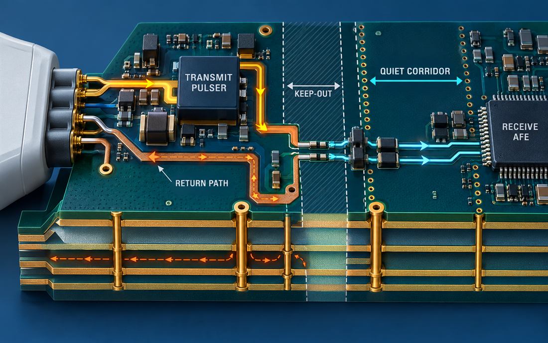
Conceptual partitioning of a probe-side pulser loop, receive AFE corridor, return path, and keep-out boundary.
Give return current a deliberate route
Designers often look at the signal trace and forget that the pulse returns through the board, connector, cable shield, decoupling network, and mechanical structure. That forgotten path is where an apparently safe layout can inject energy into the receive reference. A controlled multilayer PCB stack-up keeps the sensitive trace close to a continuous reference plane and places the pulser return where it cannot cross the AFE input corridor. The Ultrasound PCB stack-up should make that return decision visible in the cross-section. An Ultrasound PCB pulser isolation review should approve the plane pair before routing is frozen. Avoid a split directly beneath an input pair unless the complete return transition is documented and verified.
Control vias and plane transitions
Every via near the boundary should have a purpose. A return via beside a signal transition can shorten the loop, while an unplanned via field can create a capacitive bridge between noisy and quiet regions. Keep the pulser vias grouped with the pulser return. If a receive trace changes layers, place a reference-via option at the transition and check that the anti-pad pattern does not cut a slot through the receiving plane. The stack-up should be reviewed as a cross-section, not only as a top-layer screenshot.
For project management, this is a release risk because a layer change made during routing can silently invalidate an earlier noise assumption. The PCB manufacturing package should therefore include the controlled-impedance notes, via classes, drill map, and the keep-out geometry that defines the quiet corridor.
Treat the probe escape as a controlled interface
The probe connector is both an electrical interface and a mechanical datum. For an Ultrasound PCB, that datum must survive the enclosure and cable assembly review. The connector datum is part of Ultrasound PCB pulser isolation, not a cosmetic drawing detail. Its pin escape determines whether the pulser and receive paths remain separated after the enclosure, strain relief, and shield hardware are installed. A robust PCB assembly drawing identifies connector orientation, pin-one direction, shield or chassis contacts, component keep-outs, and the inspection side. Do not let an assembler decide the escape sequence from a crowded artwork file.
For a mixed-signal ultrasound PCB, the connector region should be reviewed with three overlays: the high-voltage pulse loop, the receive corridor, and the mechanical keep-out. If those overlays cannot be read on one page, the project is not ready for a pilot build. The same rule applies to a medical PCB assembly line where cable routing and fixture access can change after the first build.
Protect the receive entry
Place protection components so that they clamp the incoming event without forcing their return current through the receive amplifier reference. Keep the first sensitive node short, avoid a long exposed copper run near the switch node, and document which components may be reworked. A low-noise amplifier can be correctly selected and still underperform when the connector escape makes the board a shared antenna. This is why an ultrasound PCB material decision must be tied to geometry, not treated as an isolated purchasing choice.
Convert the concept into a manufacturing release
Before release, convert the partition into inspectable features. An Ultrasound PCB manufacturing release should expose each feature that protects the receive path. For Ultrasound PCB pulser isolation, those features include spacing, guard vias, and the reference-plane rule. A fabrication drawing should identify the plane pair used by the receive corridor, the allowed copper-to-copper spacing, the via-in-keep-out rule, and any solder-mask opening that affects the probe connector. A HDI PCB manufacturing route may help when the connector pitch is tight, but a smaller via does not automatically improve the noise result; it must still preserve the intended reference and be manufacturable at the selected build-up.
| Release item | Engineering question | Evidence to retain |
|---|---|---|
| Pulse loop | Is the high-current path compact and closed? | Top-layer overlay and return-path review |
| Receive corridor | Does the input keep one continuous reference? | Cross-section and layer-transition markup |
| Guard vias | Are they tied to the correct reference without creating slots? | Via map and fabrication note |
| Connector escape | Can assembly and inspection access the critical pins? | Assembly drawing and inspection view |
At pilot stage, the SMT assembly profile should be reviewed together with the pulser components and receive protection parts. Large thermal pads, voiding, tombstoning, or an unplanned rework loop can change the local return path. If the product needs controlled repeatability across revisions, define the approved substitute parts and the no-change zones before procurement starts.
Verify the board before the enclosure trial
Use a staged verification plan rather than waiting for a complete imaging system to reveal the problem. A production Ultrasound PCB needs this staged evidence before the enclosure trial. The final Ultrasound PCB pulser isolation check must include the cable, fixture, and shield arrangement. First inspect the bare board for the pulse loop, guard-via placement, plane continuity, and connector datum. Then check the assembled board with the intended probe fixture, cable, and shield arrangement. Exercise transmit and receive timing together; a receive-only check can miss coupling that appears only when the pulser is switching. Record the design target, fixture condition, revision, and acceptance method separately from any measured result.
The second concept image focuses on the three release checks that are easiest to miss during a fast layout review: clearance at the pulser bend, return-via placement, and solder-mask keep-out. It is a new educational diagram and not a customer measurement.
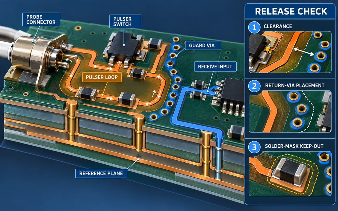
Conceptual pulser-loop inspection view with guard vias, receive entry, reference plane, and release callouts.
For a controlled handoff, ask the standard PCB capacity owner to confirm the geometry can be held, the prototype PCB assembly owner to confirm the inspection access, and the high-frequency PCB specialist to review any fast edge or controlled-impedance section. A project manager should not accept “the pulser and receive paths are separated” as a verbal statement; the release package should show the boundary, return path, and evidence for each critical feature.
Release decision
A reliable Ultrasound PCB pulser isolation plan is not defined by the number of copper layers or the price of the AFE. It is defined by whether the transmit loop, receive corridor, connector escape, reference system, and assembly controls remain understandable and repeatable across revisions. Before approving the build, confirm that the pulse return cannot cross the receive reference, that every layer transition has a return option, that the connector and shield datum are documented, and that the supplier can inspect the features that protect the echo signal. If one of those answers depends on an assumption hidden in the layout file, hold the release and close the gap before the enclosure trial.
Technical basis: Analog Devices ultrasonic front-end and MAX14808 layout guidance, Texas Instruments AFE5807 documentation, and general RF/mixed-signal PCB release practice. The ranges and checks above are engineering guidance or design targets; they must be reconciled with the selected probe, pulser, AFE, stack-up, fabrication drawing, and verification fixture.
