HomeCategory

Advanced Engineering Technologies for PCB & PCBA Solutions - KKPCB

RO4835™ Laminate Data Sheet High Frequency PCB Materials

As electronic systems continue moving toward higher frequencies, faster signal transmission, and more demanding operating environments, PCB material selection has become a critical factor affecting product performance. For RF, microwave, automotive radar, and high-speed communication applications, conventional FR-4 materials may not always provide sufficient electrical stability due to higher dielectric loss and variations in dielectric...

What is a high-frequency PCB? You must know about high-frequency and high-speed PCB

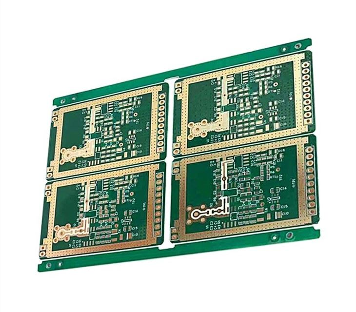
Do you know what high-frequency PCB is ? What applications are high-frequency PCB used for? Today, the editor of United Multilayer will show you what high-frequency PCB is and in what fields it is used. High-frequency PCB is a special circuit board with a higher electromagnetic frequency, which is above 1GHz. The physical properties, precision and technical...

How to distinguish whether a PCB is single-layer or double-layer?

PCB physical object: A double-layer board has copper foil conductors on both sides. Electronic version PCB: There are two colors of conductors (different colors of conductors represent different layers) 3 Double-layer PCB board design and wiring principles The ground wire of the double-layer board is designed to be formed as a grid-shaped frame, that is, more parallel ground wires are laid...

Comprehensive Electronic Components Sourcing Service at KKPCB

In modern electronic product development, PCB manufacturing and PCBA assembly are no longer limited to board fabrication and component placement. A stable and efficient electronic components sourcing strategy has become a critical factor affecting project schedules, production costs, and product reliability. Component shortages, supply chain uncertainty, counterfeit risks, and inconsistent quality can create significant challenges...

PCB design technologySetting Up the PCB Design Software Environment: A Comprehensive GuidePCB design technology

Software Rule Settings To begin with, enter Design > Rules and adjust the options based on design requirements: Safety Spacing Settings: In PROTEL99SE, the Clearance Constraint under Routing defines the necessary spacing between traces, pads, and vias of different networks. Single/Double-sided boards: Set spacing to 10-12mil. Multi-layer boards (four layers or more): Set spacing to 6-8mil. Routing Layer and Direction: Go to Routing Layers under Routing and set...

4 Special Electroplating Methods in Circuit Board Welding

In PCB circuit board manufacturing, various electroplating methods are employed to enhance performance, durability, and contact quality. This article focuses on four specialized electroplating methods commonly used in PCB (printed circuit board) welding processes. 1. Finger-Ring Electroplating Finger-ring electroplating involves plating rare metals, such as gold, on the edge connectors or gold fingers of circuit boards to...

8 Common Circuit Design Mistakes That Affect PCB Performance and Reliability

Introduction In electronic product development, many design decisions are based on common assumptions or long-established practices. However, as circuits become: faster, smaller, more power-sensitive, more integrated, some traditional design approaches may create unexpected problems during validation, manufacturing, or mass production. Issues such as: unnecessary PCB complexity, increased power consumption, signal instability, higher manufacturing costs, reduced...

Understanding and Improving PCB Open Circuits: Causes and Solutions

Why PCB Open Circuits Matter In PCB manufacturing and PCB assembly, PCB open circuits are one of the most common and critical defects affecting electrical performance and product reliability. An open circuit occurs when an electrical path is unintentionally broken, preventing current from flowing through the circuit. For industries requiring high reliability—such as automotive electronics,...

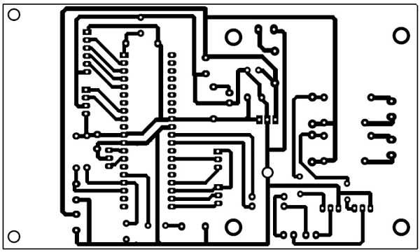
PCB Drawing: A Summary of Key Practices from Years of Experience

PCB drawing is a critical stage in electronic product development that transforms circuit concepts and schematic designs into physical circuit boards. Although modern PCB design software has significantly improved design efficiency, creating a reliable PCB drawing still requires extensive engineering experience. A PCB layout must not only achieve electrical connections but also consider signal integrity,...

Key Grounding Techniques in Electronic Design

Grounding is one of the most fundamental elements in electronic system design. A well-designed grounding structure provides a stable reference potential, ensures reliable current return paths, reduces electrical noise, and improves overall system performance. As electronic products continue developing toward higher operating frequencies, faster data transmission, and increased integration, grounding design has become more challenging....