
Introduction
In electronic product development, many design decisions are based on common assumptions or long-established practices.
However, as circuits become:
- faster,
- smaller,
- more power-sensitive,
- more integrated,
some traditional design approaches may create unexpected problems during validation, manufacturing, or mass production.
Issues such as:
- unnecessary PCB complexity,
- increased power consumption,
- signal instability,
- higher manufacturing costs,
- reduced product reliability
often originate from small design decisions made during the early development stage.
This article discusses eight common circuit design misunderstandings and explains how engineers can optimize PCB performance through better design practices.
Misunderstanding 1: Thin Traces and Automatic Routing Are Always Suitable for Simple PCB Designs
Reality:
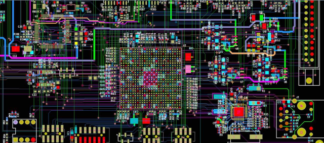
Automatic routing tools can improve design efficiency, but relying entirely on them may create unnecessary manufacturing challenges.
Although narrow traces and dense routing may appear acceptable for low-complexity designs, they can lead to:
- increased PCB area,
- excessive via usage,
- longer signal paths,
- more complicated manufacturing processes.
From a PCB manufacturing perspective, factors such as:
- trace width,
- via quantity,
- layer utilization,
- drilling complexity
directly affect production cost and yield.
Better Approach:
Manual routing optimization is still valuable, especially for:
- power distribution networks,
- high-speed signals,
- sensitive analog circuits,
- RF transmission lines.
A well-optimized layout can reduce:
- unnecessary vias,
- signal interference,
- fabrication difficulty,
while improving overall production reliability.
Misunderstanding 2: Every Bus Signal Requires Pull-Up or Pull-Down Resistors
Reality:
Pull-up and pull-down resistors are important for defining signal states, but adding them unnecessarily may increase power consumption.
For example:
- large digital buses,
- memory interfaces,
- FPGA connections,
may contain dozens of signals.
If every line includes additional resistors, the combined current consumption can become significant.
Potential issues include:
- increased standby power,
- unnecessary heat generation,
- higher component count.
Better Approach:
Engineers should analyze:
- signal requirements,
- leakage current,
- interface specifications,
- operating conditions
before adding termination resistors.
Proper resistor selection helps achieve a balance between:
- signal stability,
- power efficiency,
- BOM optimization.
Misunderstanding 3: Unused I/O Pins Can Be Left Floating Without Consequences
Reality:
Unused input pins should not always be left floating.
Floating I/O pins, especially on:
- MCUs,
- CPUs,
- FPGAs,
may become unstable due to electrical noise or external interference.
This can cause:
- unnecessary switching activity,
- increased current consumption,
- unpredictable system behavior.
Better Approach:
Unused pins should be configured properly according to device recommendations.
Common solutions include:
- setting unused pins as outputs,
- applying pull-up or pull-down configurations,
- disabling unused functions.
Proper pin management improves:
- system stability,
- power efficiency,
- long-term reliability.
Misunderstanding 4: Maximizing FPGA Resource Utilization Always Improves Design Efficiency
Reality:
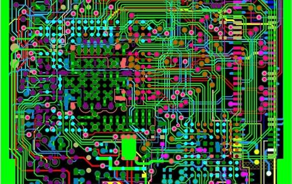
Higher FPGA utilization does not always mean better performance.
Although using more available logic resources may reduce device cost, it can significantly increase:
- dynamic power consumption,
- thermal generation,
- design complexity.
Power consumption depends not only on:
- logic utilization,
but also on:
- switching frequency,
- clock activity,
- flip-flop usage,
- operating voltage.
Better Approach:
FPGA designs should focus on optimization rather than maximum utilization.
Engineers should consider:
- clock gating,
- reducing unnecessary switching,
- optimizing high-speed logic paths,
- balancing performance and power.
Misunderstanding 5: Small ICs Always Consume Very Little Power
Reality:
Physical size does not directly determine power consumption.
Some small devices may consume significant power when driving external loads.
For example:
- buffer ICs,
- drivers,
- interface components
may have low standby current but much higher consumption during operation.
Factors affecting power include:
- output current,
- switching frequency,
- capacitive loading,
- operating voltage.
Better Approach:
Power estimation should consider actual operating conditions rather than only datasheet standby values.
Engineers should evaluate:
- active current,
- switching behavior,
- thermal impact,
- system workload.
Misunderstanding 6: Permanently Activating Chip Select Improves Memory Performance
Reality:
Keeping the chip select (CS) signal permanently active may seem like a way to reduce access delay, but it can significantly increase power consumption.
When memory devices remain continuously enabled:
- standby current increases,
- thermal stress may rise,
- battery life may decrease.
Better Approach:
Optimize memory control timing by:
- minimizing unnecessary access cycles,
- controlling CS signals properly,
- using low-power memory modes when available.
For portable and battery-powered systems, efficient memory management is especially important.
Misunderstanding 7: All Signal Overshoot Problems Must Be Eliminated Through Termination Matching
Reality:
Overshoot and ringing are common phenomena in high-speed circuits.
The goal is not always to eliminate them completely, but to keep them within acceptable limits.
Over-designing termination networks may introduce:
- unnecessary power loss,
- reduced signal amplitude,
- additional components,
- increased PCB complexity.
Better Approach:
Signal integrity optimization should focus on:
- impedance control,
- rise/fall time analysis,
- trace length management,
- return path design.
Simulation tools can help determine whether termination is actually required.
Misunderstanding 8: Power Optimization Is Only a Hardware Design Responsibility
Reality:
Power efficiency depends on both hardware and software decisions.
Hardware determines:
- circuit efficiency,
- leakage current,
- power distribution.
Software controls:
- processor activity,
- memory access frequency,
- peripheral usage.
Poor software optimization can cause unnecessary hardware power consumption.
Better Approach:
A complete low-power strategy should combine:
Hardware Optimization
Including:
- efficient PCB layout,
- optimized power distribution network,
- low-power components,
- proper thermal design.
Software Optimization
Including:
- reducing unnecessary memory access,
- improving cache utilization,
- optimizing interrupt handling,
- managing sleep modes.
How PCB Design Practices Influence Product Performance
Many circuit-level decisions eventually affect PCB manufacturing and product reliability.
During PCB design review, engineers should consider:
Signal Integrity
- impedance control
- return path optimization
- noise reduction
Power Integrity
- PDN design
- voltage stability
- thermal management
Manufacturing Feasibility
- trace spacing
- via structures
- component accessibility
- testability
Reliability
- EMI control
- thermal stress
- mechanical durability
Early engineering review helps identify hidden risks before prototype production.
Conclusion
Circuit design is not only about making a system function — it is about creating a product that can achieve:
- stable performance,
- efficient power consumption,
- reliable manufacturing,
- long-term operation.
Many PCB issues originate from assumptions that appear reasonable but may not fit modern high-speed and highly integrated electronics.
By understanding these common design misunderstandings and applying engineering-driven optimization, designers can reduce development risks and improve product readiness.
At KKPCB, our engineering team supports customers from PCB fabrication and PCBA assembly to DFM analysis, helping identify potential design and manufacturing challenges before production.
