
PCB drawing is a critical stage in electronic product development that transforms circuit concepts and schematic designs into physical circuit boards.
Although modern PCB design software has significantly improved design efficiency, creating a reliable PCB drawing still requires extensive engineering experience. A PCB layout must not only achieve electrical connections but also consider signal integrity, power distribution, thermal performance, manufacturability, and long-term reliability.

Many issues discovered during PCB fabrication or product testing originate from early PCB drawing decisions, such as improper component placement, insufficient spacing, poor grounding structures, or designs that exceed manufacturing capabilities.
Therefore, following proven PCB drawing practices can help reduce development risks, improve production efficiency, and ensure a smoother transition from prototype to mass production.
1. Understand the Schematic Before Starting PCB Drawing
Before beginning PCB layout, engineers should fully understand the circuit functionality and design requirements.
Important information to review includes:
- Circuit architecture
- Power supply structure
- Signal flow
- Component functions
- Critical signal paths
- Interface requirements
A clear understanding of the schematic helps designers make better decisions regarding:
- Component placement
- Layer allocation
- Routing strategy
- Grounding structure
Starting PCB drawing without sufficient circuit understanding may result in repeated modifications and potential reliability issues.
2. Plan PCB Layer Stack-Up Properly
For multilayer PCB designs, stack-up planning should be completed before routing.
The layer structure directly affects:
- Signal integrity
- Power distribution
- EMI performance
- Manufacturing reliability
Common considerations include:
Signal Layer Arrangement
High-speed signal layers should be placed close to reference planes to maintain stable transmission characteristics.
Power and Ground Layer Design
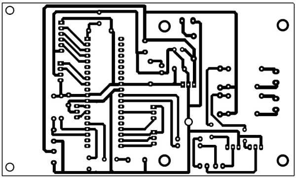
Dedicated power and ground layers provide:
- Lower impedance paths
- Better current distribution
- Reduced noise coupling
Material Selection
The PCB material should match application requirements.
Examples:
- FR-4 for general electronic products
- Low-loss materials for RF/high-speed applications
- Flexible materials for compact or bending applications
3. Component Placement Optimization
Component placement is one of the most important steps in PCB drawing.
A good layout should consider both electrical performance and manufacturing requirements.
3.1 Functional Area Separation
Components should be grouped according to their functions.
Typical areas include:
- Power supply section
- Digital processing section
- Analog circuit section
- Communication interface section
- RF circuit section
This helps reduce interference and simplifies routing.
3.2 Signal Flow Consideration
Component placement should follow the signal transmission path.
Benefits include:
- Shorter routing distance
- Reduced signal loss
- Improved debugging efficiency
Critical components should be placed close to related circuits.
3.3 Thermal Management
Heat-generating components require special attention.
Examples:
- Power ICs
- Voltage regulators
- High-current devices
Consider:
- Copper area
- Thermal vias
- Heat dissipation paths
Poor thermal design may reduce product reliability.
4. PCB Routing Practices
Routing quality directly affects PCB performance.
4.1 Keep Critical Signal Paths Short
Important signals include:
- Clock signals
- High-speed data lines
- Analog measurement signals
- RF signals
Short and optimized routing helps reduce:
- Signal delay
- Noise interference
- Transmission loss
4.2 Maintain Signal Integrity
For high-speed PCB designs, engineers should consider:
- Controlled impedance
- Differential pair routing
- Trace length matching
- Reference plane continuity
Improper routing may cause:
- Reflection
- Crosstalk
- Signal distortion
4.3 Power and Ground Routing
Power traces should be designed according to current requirements.
Important considerations:
- Trace width
- Voltage drop
- Return current path
- Ground connection quality
A reliable grounding structure is essential for stable system operation.
5. Design for Manufacturing (DFM) Considerations
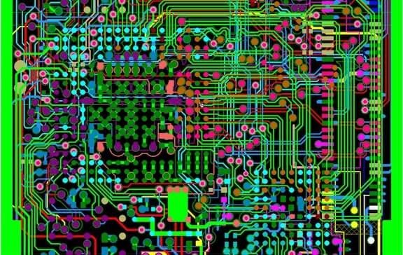
A PCB drawing should always consider manufacturing feasibility.
Key DFM factors include:
5.1 Trace Width and Spacing
Design rules should match fabrication capabilities.
Incorrect settings may lead to:
- Open circuits
- Short circuits
- Reduced production yield
5.2 Via Design
Via structures should consider:
- Hole size
- Aspect ratio
- Via spacing
- Reliability requirements
For HDI and high-density designs, microvia reliability becomes especially important.
5.3 Component Assembly Requirements
PCB drawings should consider:
- Component package size
- SMT placement requirements
- Soldering process
- Inspection accessibility
Good assembly design helps improve production efficiency.
6. Pay Attention to EMC and EMI Control
Electromagnetic compatibility should be considered during PCB drawing.
Common practices include:
Reduce Current Loop Area
Smaller loops help reduce electromagnetic radiation.
Separate High-Noise and Sensitive Circuits
Examples of noisy circuits:
- Switching power supplies
- Motor drivers
- High-current circuits
Sensitive circuits include:
- Sensors
- Analog amplifiers
- Communication receivers
Optimize Ground Structures
Continuous ground planes and proper via placement help improve EMC performance.
7. Testing and Debugging Considerations
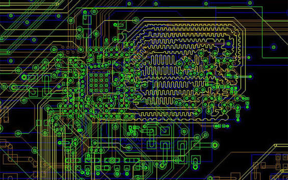
A professional PCB drawing should consider future testing requirements.
Important design elements include:
Test Points
Test points support:
- Production inspection
- Debugging
- Maintenance
Programming and Debug Interfaces
For MCU-based boards, ensure:
- Programming interfaces are accessible
- Debug signals are properly routed
Functional Testing Requirements
PCB design should support:
- ICT testing
- Functional testing
- Electrical verification
Early consideration reduces production troubleshooting difficulties.
8. Common PCB Drawing Mistakes
Incorrect Component Orientation
Incorrect placement may:
- Increase assembly difficulty
- Cause production errors
Insufficient Clearance
Poor spacing may result in:
- Electrical safety risks
- Assembly problems
Ignoring Manufacturing Limitations
Designs exceeding manufacturing capability may lead to:
- Low yield
- Additional costs
- Production delays
Poor Grounding Design
Improper grounding may cause:
- Noise problems
- Signal instability
- EMI issues
9. Importance of Design Review Before Fabrication
Before releasing PCB files for production, engineers should perform a complete review.
Recommended checks include:
- Design Rule Check (DRC)
- Electrical Rule Check (ERC)
- DFM review
- Stack-up verification
- Signal integrity analysis
Early review helps identify potential issues before manufacturing.
Conclusion
PCB drawing is not simply the process of connecting components according to a schematic. It is a comprehensive engineering task involving electrical performance, mechanical design, manufacturing capability, and reliability considerations.
Years of PCB development experience show that successful designs require attention to details such as layer planning, component placement, routing strategy, grounding structure, thermal management, and DFM optimization.
By applying practical PCB drawing principles during the design stage, engineers can reduce development risks, improve production yield, and create more reliable electronic products.
