
A Healthcare PCB for ECG monitoring may pass a bench check with a short laboratory lead and still become noisy when the production patient cable is attached. The production cable changes pickup area, shield current, connector parasitics, and the route by which common-mode energy reaches the analog front end. This is a design-review scenario for a Healthcare PCB for ECG monitoring, not a reported customer project or measured KKPCB result. It shows how a Healthcare PCB should be reviewed as a complete input system rather than as a quiet IC surrounded by a few filter parts.
For a Healthcare PCB for ECG monitoring, the practical question is not simply “which filter value should be changed?” It is whether the electrode path, enclosure interface, reference return, power conversion, and assembly process preserve the conditions assumed by the measurement circuit. A Healthcare PCB that routes the connector and the ECG analog front end without a documented boundary can make later EMC debugging expensive and ambiguous.
Healthcare PCB for ECG: patient-lead routing before filter tuning
Begin at the connector pins and follow each electrode input through protection, series impedance, filtering, and the AFE input. Keep the paired paths geometrically comparable: asymmetric trace length, different via count, unequal filter placement, or a nearby fast digital edge can convert interference that was common to both inputs into a differential error. The patient-lead connector boundary also deserves mechanical review. Shield termination, shell bonding, strain relief, and the enclosure opening determine where cable current returns; they are not details to defer until after routing.
Place the first protection and filter components close to the connector or the AFE according to the selected protection topology and the device vendor’s reference design. The important criterion for this Healthcare PCB is a short, controlled path with a deliberate return, not a universal placement rule. Avoid unused stubs and unnecessary test pads on high-impedance nodes. A test point can add capacitance and act as a pickup structure; if access is essential, include it in the input-capacitance and noise review instead of treating it as electrically invisible.
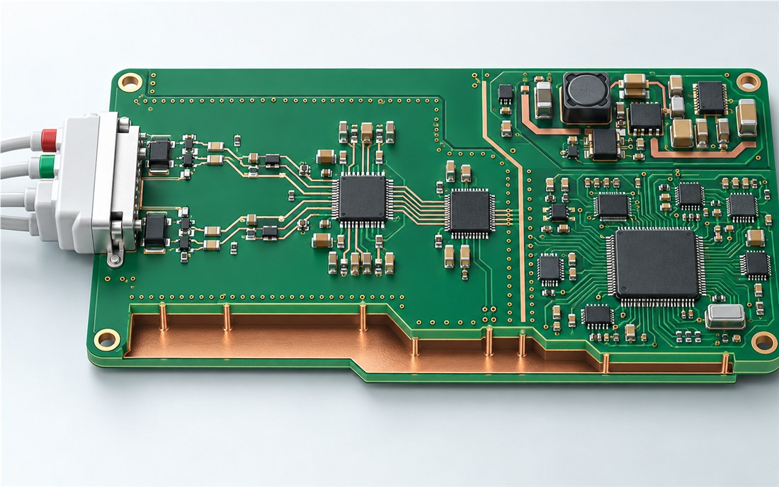
Keep the return architecture coherent across mixed-signal zones
A split-looking floorplan is not automatically a good grounding plan. The AFE, ADC interface, clock source, display, radio, and switching regulator need intentional placement so their return currents do not cross the electrode reference region. Use a continuous reference plane where the architecture permits it, and keep high-edge-rate clocks and converter switch nodes away from the input corridor. If a plane cut or chassis boundary is required, document how each signal crosses it and where its return closes.
For a multilayer stack, reserve an uninterrupted reference adjacent to sensitive signal routing and review layer transitions as current loops, not just as via counts. A mixed-signal multilayer PCB can reduce loop area when the layer assignment is consistent; simply adding layers does not cure poor partitioning. Keep the input pair away from the regulator’s hot loop, inductor field, display flex, and radio feed. Place decoupling at the relevant AFE and converter supply pins, then verify that return vias actually connect to the intended plane.
On a Healthcare PCB, common-mode feedback or a driven reference can help only when the device architecture, electrode configuration, protection network, and safety design support it. Do not route a driven output beside the input pair or use it as a substitute for cable-shield strategy. The Healthcare PCB prototype review should include both the electrical schematic and the physical connector/cable arrangement, because the bench fixture can hide the very coupling path that appears in the final enclosure.
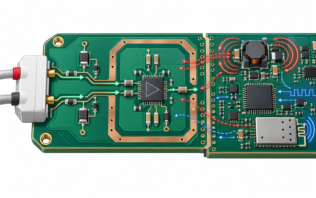
Turn a noise complaint into a controlled verification plan
When the reported symptom is a wandering baseline, mains-frequency pickup, or bursts synchronized to radio or display activity, log the conditions before changing the layout. Record lead configuration, cable type and length, enclosure state, battery or adapter power, firmware activity, filter population, and test setup. A useful comparison matrix varies one factor at a time: cable attached versus shorted input, radio idle versus transmitting, display static versus refreshing, and charger disconnected versus connected. These are proposed engineering checks, not results claimed for a KKPCB build.
ADI’s CN-0308 notes that an ECG surface signal is typically around 1 mV and discusses system-level noise budgets, including a 30 μV peak-to-peak limit cited for applicable requirements; the actual acceptance criterion must be taken from the target device specification and applicable standard, not copied blindly. TI’s ADS129x documentation and ECG front-end notes provide device-specific information on input filtering, lead-off detection, and common-mode management. FDA EMC guidance emphasizes evaluating emissions and immunity in the device’s intended environment. Together, these references support a verification plan that includes both the analog signal path and system-level disturbance conditions.
Protect the design through fabrication and assembly release
Before release, provide the fabricator with the approved stackup, copper weights, controlled-impedance requirements where applicable, and the exact revision of the input-area Gerbers. Ask for a manufacturability review of connector pitch, solder-mask webs, via-to-pad clearances, and any shield or chassis connection. A focused PCB design-for-manufacturing review helps prevent a late tooling or footprint change from shifting the patient-input geometry after the electrical review.
For a Healthcare PCB for ECG monitoring, protect high-impedance areas from residue and handling damage at assembly. Define polarity and orientation for protection components, keep-clean requirements if they are part of the validated process, and inspection access for fine-pitch AFE packages. Specify whether the build is prototype-only or intended to represent the production solder process. A Healthcare PCB prototype should use the intended connector, cable, enclosure, and major power components whenever possible; otherwise the team is validating a fixture, not the final boundary.
For the project manager, the Healthcare PCB for ECG release package should identify the exact board revision, BOM alternates, AFE configuration, firmware build, test fixture, cable, and acceptance limits. Keep the electrical verification record separate from manufacturing inspection records for every Healthcare PCB revision. If a component substitution changes input leakage, capacitance, protection behavior, or power-supply noise, route it through formal change review rather than treating it as a purchasing-only equivalent. The prototype assembly workflow and SMT assembly controls should preserve the approved revision and traceability.
Practical release checklist
- Map each electrode from connector contact to AFE pin, including protection and filter components.
- Confirm pair symmetry, reference-plane continuity, and return closure at every layer transition.
- Review shield, enclosure, cable strain relief, and patient lead configuration as one system boundary.
- Test the same cable, enclosure, power mode, and radio/display activity expected in the product use case.
- Freeze the BOM, board revision, firmware, fixture, and acceptance criteria together before the next build.
In short, a Healthcare PCB for ECG capture is a boundary-control problem as much as an amplifier-selection problem. The Healthcare PCB project succeeds when the cable, return path, analog partition, assembly process, and verification setup are released as one traceable configuration. For a new revision, a medical cable-interface assembly, manufacturing review, and design-validation prototype should all use the same controlled files.
The final outgoing quality inspection should follow the approved inspection plan and must not be treated as a substitute for system-level ECG and EMC verification.
Sources: Analog Devices, CN-0308 “Powering an ECG Front End in Battery Powered Patient Monitoring Applications” (typical signal scale and system-level noise discussion); Texas Instruments, ADS129x datasheet and “Analog Front-End Design for ECG Systems Using Delta-Sigma ADCs” (device-specific front-end guidance); U.S. FDA, “Electromagnetic Compatibility (EMC) of Medical Devices” (intended-use EMC assessment). Values and recommendations are context-dependent; no customer measurement or KKPCB test result is represented here.

