
A wearable monitor puts a radio, battery, sensor front end, and human-body interface into a very small enclosure. That makes the Healthcare PCB a mixed-signal and RF integration problem: antenna performance depends on the board and enclosure, while the ECG or optical acquisition path must remain stable as the radio transmits and the power system changes state. TI’s TIDA-01580 is a useful example of a wearable design that combines ECG and PPG sensing with Bluetooth and a board antenna. Its layout is a reference case, not a universal wearable template.
Map the Healthcare PCB sensing, radio, and power domains
Begin with a block diagram that follows actual currents and signals, not just component categories. Mark the patient or electrode connector, high-impedance input network, analog front end, processor, radio, antenna feed, battery, charging path, display or haptic loads, and every switching converter. Note which connections run through flex tails or external cables. A Healthcare PCB floorplan can then separate vulnerable inputs from transmit-current loops while preserving a short, well-defined RF route.
Keep the intended signal return beside each signal. A ground pour is not automatically a quiet return if a radio burst or converter pulse shares the same narrow copper neck. Likewise, an arbitrary split plane can force return current around a gap and increase loop area. Define the reference domains from the circuit and stackup, then review where their currents meet at connectors, stitching vias, and power entry. A multilayer PCB stackup should make the intended RF reference and sensitive analog return visible layer by layer.
For ECG, inspect the complete electrode-to-amplifier path, including protection devices, bias or driven-reference circuitry, and lead-off detection. For optical sensing, identify LED drive currents, photodiode input nodes, and the receiver return path. These circuits have different susceptibility paths, so a Healthcare PCB review should use the actual front-end schematic and product use case. A focused Healthcare PCB design review can connect the schematic map to the physical placement before routing is locked. A Healthcare PCB should retain that domain map through assembly and test.
Reserve the antenna region before routing
Choose the radio module or transceiver, antenna type, enclosure material, battery position, and intended body-worn orientation early enough to reserve the antenna region. Printed antennas, chip antennas, and module antennas have different ground and clearance needs. The vendor reference layout is a starting point for that exact antenna system; its geometry cannot be copied blindly onto a different laminate, layer count, enclosure, or board outline.
Place the antenna where the enclosure leaves a plausible radiation path, away from a metal battery can, display frame, shield, dense connector cluster, or body-facing absorber when the selected design guidance requires it. Define the no-copper and component keepouts from the chosen antenna documentation. Then check the enclosure, wrist strap, patient lead, adhesive, and nearby plastics as part of the antenna system. This rigid-flex PCB assembly discussion should include how the flex bend, stiffener, and housing affect the antenna’s installed position. A PCB fabrication review should also check whether panel and edge tolerances preserve that location.
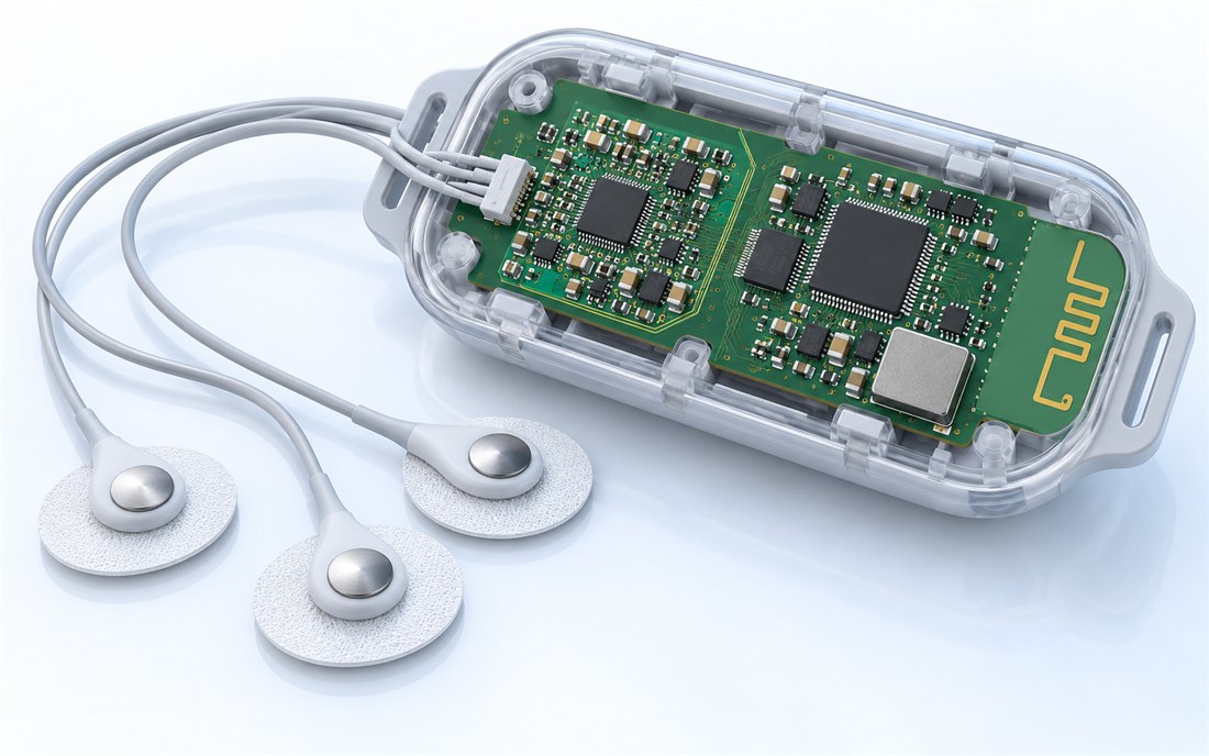
Do not treat antenna keepout as a decorative outline. Extend its rules to every copper layer, component body, screw, shield, and nearby cable that can change the electromagnetic environment. If an inner-layer clearance is required around the antenna or matching components, show it in the CAD constraints and fabrication view instead of relying on memory. A manufacturing PCB design-for-manufacturing review can flag conflicts between the antenna zone, panel rails, tooling features, and mechanical edge tolerances.
Control the RF feed and matching network
Route the radio-to-antenna feed using the impedance target and geometry supported by the selected radio vendor, stackup, and field solver or design tool. A controlled-impedance callout needs the dielectric thickness, copper weight, reference plane, line width, spacing, and finished construction that produced the target. Keep the feed short and consistent, avoid unnecessary stubs, and place matching parts in the recommended order near the antenna feed point. Do not insert a ground split beneath a transmission path if the design expects a continuous reference.
Nordic’s nRF52832 reference-circuit guidance, for example, describes a ground-plane arrangement and an inner-layer keepout beneath its antenna matching circuitry. Those instructions are device-specific. If you use another radio or antenna, use that product’s own reference and validate the assembled design. A PCB prototype can help measure the actual feed and antenna response before design release, but measurements need a documented board revision, enclosure, test cable, and calibration setup.
Keep tuning components accessible in the early prototype when the design flow calls for tuning. Record the fitted values, antenna part number, board revision, solder-mask condition, and enclosure state for each measurement. When tuning is complete, lock the approved values and footprint option in the released BOM and assembly drawing. A prototype assembly build is most useful when it represents the intended battery, display, flex, and housing stack rather than a bare board alone.
Protect quiet sensor inputs from changing currents
Radio transmit bursts and converter switching can couple into a sensor path through shared impedance, electric or magnetic fields, supply ripple, common-mode conversion, or the patient lead itself. Distance helps only when it changes a real coupling path. Review the antenna feed and matching network, power inductor, fast switch node, clock fanout, sensor input, and cable connector as a coupled system. Route high-impedance input pairs together, keep their reference predictable, and avoid running them beside a high-current pulsed path for long distances.
Place local decoupling where the IC supply current enters and returns. Trace the return path through the actual plane and vias, then check whether burst current crosses a narrow neck shared with analog reference or sensor bias. Review charger, battery boost, display refresh, status LEDs, and haptic motor states even if each is inactive during the radio’s typical data transfer. Their simultaneous or sequenced behavior should match the firmware and power policy. A Healthcare PCB build should preserve the intended component orientation, ground connections, and shield contacts that the layout review assumes.
Where the circuit supports it, test whether sampling during radio activity produces a repeatable change in noise or data quality. Compare radio-off and radio-on states under the same electrode simulator or optical input, cable, battery voltage, and load condition. This is a verification plan for that board and device configuration, not a certification result. A wearable PCB prototype review should capture the stimulus, firmware state, test instruments, and raw observations so a design change can be compared honestly. A PCB assembly prototype build can include the intended flex and housing during that evaluation.
Verify radio and battery operating modes together
Build a verification matrix around the real operating modes: advertising, connection interval, packet activity, reconnection, sensor acquisition, LED pulse sequence, display update, charging, and low-battery behavior. Record whether the radio transmits continuously, in short bursts, or at a duty cycle defined by the application. Check wireless range and packet behavior in the intended enclosure and orientation while observing the sensor path under a repeatable electrical or optical input. A single open-air range test does not represent every body-worn position or clinical environment.
The FDA’s wireless-medical-device resources call out selection of wireless technology, quality of service, coexistence, security, and EMC as areas for manufacturers to consider. Use the applicable product risk process to select representative interferers, distances, channels, traffic patterns, and acceptance criteria. The board team can contribute antenna and emissions evidence, but the product manufacturer owns system-level conclusions and any regulatory submission. For a Healthcare PCB, preserve the exact test configuration with the design record.
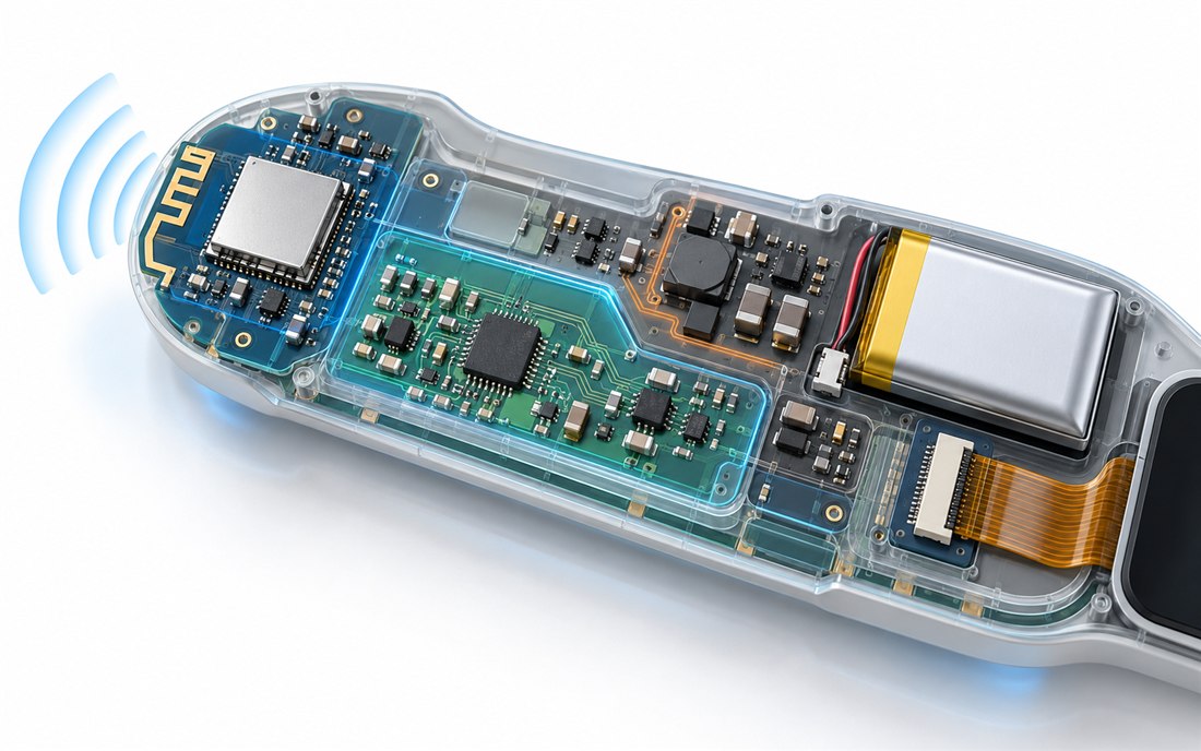
Use current probes or voltage measurements only where the probe setup will not create a new antenna or ground path. Document instrument bandwidth, probe connection, cable routing, radio settings, battery state, and the sensor stimulus. If a problem follows the battery or charger state, investigate the supply and return path; if it follows antenna orientation or cable position, investigate the installed RF and common-mode paths. A PCB engineering design review should turn each observed symptom into a testable layout or system hypothesis.
Release a repeatable wearable PCB build
Before release, include the full layer stack, controlled-impedance requirements, antenna keepouts, matching-network reference designators, component orientation, approved alternates, board-edge tolerances, and flex or stiffener details where used. State which measurements are required on first articles and which changes require RF revalidation. Make sure solder mask, copper finish, panelization, depanelization, and enclosure features match the configuration used for antenna and coexistence checks.
Track the radio, antenna, battery, front-end, and enclosure revisions as one configuration. If an alternate radio module or antenna is proposed, review its footprint, pinout, keepout, matching network, firmware settings, and test plan before approval. A PCB prototype assembly review can expose access and fit issues, while the approved release package remains the authority for subsequent production. For a Healthcare PCB, traceability helps keep measured performance attached to the board and enclosure that were actually evaluated.
In short, wearable RF performance and quiet sensing need a shared floorplan, a controlled feed, explicit return paths, and verification across representative operating modes. Start from the selected radio and sensor references, adapt them to the product’s board and housing, and document every validated change. A Healthcare PCB review is strongest when the RF, analog, mechanical, firmware, and manufacturing teams agree on the same released configuration.
Sources: Texas Instruments TIDA-01580 wearable wireless ECG/SpO2/PTT reference design, including its reference PCB antenna and downloadable design files; Nordic Semiconductor nRF52832 reference circuitry and PCB guidelines, for device-specific RF path and antenna matching guidance; U.S. FDA Wireless Medical Devices, for wireless coexistence and risk-management context. These references do not establish performance or compliance for a different board.

