
Grounding is one of the most fundamental elements in electronic system design. A well-designed grounding structure provides a stable reference potential, ensures reliable current return paths, reduces electrical noise, and improves overall system performance.

As electronic products continue developing toward higher operating frequencies, faster data transmission, and increased integration, grounding design has become more challenging. Improper grounding methods may lead to:
- Signal interference
- Electromagnetic interference (EMI)
- Ground loops
- Signal integrity degradation
- System instability
In modern PCB design, grounding is not simply connecting all ground points together. Engineers need to consider current flow, frequency characteristics, circuit structure, and application requirements to select an appropriate grounding strategy.
1. The Importance of Grounding in Electronic Design
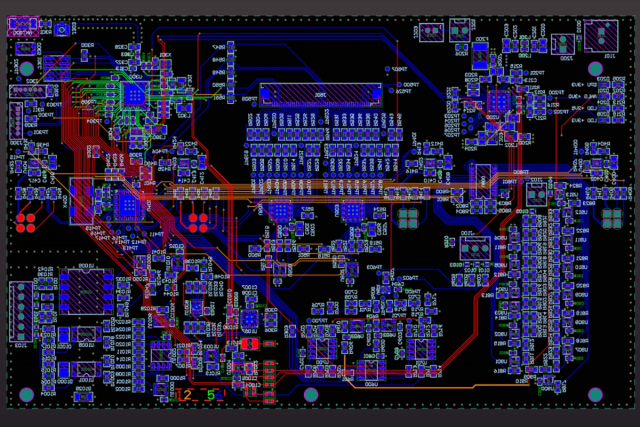
Grounding performs several important functions in electronic systems.
1.1 Providing a Stable Voltage Reference
Electronic circuits require a stable reference point for accurate operation.
A poor grounding system may introduce:
- Voltage fluctuations
- Measurement errors
- Signal distortion
Sensitive circuits such as analog sensors and communication modules are particularly affected by ground noise.
1.2 Providing Current Return Paths
Current must always have a complete return path.
At low frequencies, current generally follows the path of least resistance. However, at high frequencies, current follows the path of least impedance.
Therefore, PCB grounding design must consider:
- Return current paths
- Loop areas
- Parasitic inductance
1.3 Reducing EMI and Noise
Uncontrolled current loops can generate electromagnetic radiation.
Proper grounding helps:
- Reduce noise coupling
- Minimize radiation
- Improve EMC performance
This is especially important in high-speed digital systems and RF applications.
2. Common Grounding Techniques in Electronic Design
Different electronic systems require different grounding strategies.
2.1 Single-Point Grounding
Single-point grounding connects different circuit sections to one common grounding point.
This method is commonly used in:
- Low-frequency analog circuits
- Audio systems
- Precision measurement equipment
Advantages:
- Reduces ground loop problems
- Prevents unwanted current interaction
- Improves measurement accuracy
Limitations:
At high frequencies, long grounding connections may introduce additional inductance, reducing effectiveness.
2.2 Multi-Point Grounding
Multi-point grounding connects multiple grounding locations directly to a common ground structure.
It is widely used in:
- Digital systems
- High-frequency circuits
- Communication equipment
Advantages:
- Reduces grounding impedance
- Improves high-frequency performance
- Provides better noise control
For high-speed PCB designs, multi-point grounding is often combined with continuous ground planes.
2.3 Ground Plane Design
In multilayer PCB design, dedicated ground planes are one of the most effective grounding methods.
A continuous ground plane provides:
- Low impedance return paths
- Improved signal integrity
- Reduced EMI radiation
- Better power integrity
High-speed signals should generally be routed close to a reference ground plane to maintain stable electrical characteristics.
3. Analog and Digital Grounding Techniques
Modern electronic systems often include both analog and digital circuits.
Digital circuits generate switching noise, while analog circuits require a clean reference environment.
Common approaches include:
- Analog ground (AGND)
- Digital ground (DGND)
- Power ground (PGND)
3.1 Ground Separation
Separating different ground areas can help reduce noise coupling.
Typical applications include:
- Sensor systems
- Data acquisition equipment
- Mixed-signal circuits
However, improper ground separation may create:
- Longer return paths
- Increased EMI
- Signal integrity problems
Ground separation should be based on actual current flow analysis.
3.2 Single Connection Point Between Grounds
In some mixed-signal designs, analog and digital grounds are connected at a carefully selected point.
The purpose is to:
- Prevent unwanted current circulation
- Maintain signal reference consistency
The connection location depends on circuit architecture and operating frequency.
4. Grounding Techniques for High-Speed PCB Design
High-speed circuits have strict grounding requirements.
Important considerations include:
4.1 Maintain Continuous Return Paths
When high-speed signals pass through different PCB areas, their return current should have a continuous path.
Avoid:
- Ground plane gaps
- Unnecessary layer transitions
- Split reference planes
4.2 Reduce Current Loop Areas
Smaller loop areas help reduce:
- Electromagnetic radiation
- Noise coupling
- Signal distortion
Recommended practices:
- Place decoupling capacitors close to IC power pins
- Keep power and ground connections short
- Optimize component placement
4.3 Ground Via Optimization
Ground vias are essential for connecting different ground layers.
Proper via placement helps:
- Reduce impedance
- Improve shielding
- Enhance high-frequency grounding performance
Common applications include:
- RF circuits
- High-speed interfaces
- Multilayer PCBs
5. Grounding Techniques for RF and Microwave Circuits
RF and microwave circuits are highly sensitive to grounding quality.
At high frequencies, even small grounding imperfections can affect circuit performance.
Key techniques include:
Ground Via Fence
A series of grounding vias around RF transmission lines helps:
- Improve electromagnetic isolation
- Reduce signal leakage
- Control RF current paths
Solid Ground Reference
RF circuits require stable ground structures to maintain:
- Impedance consistency
- Signal integrity
- Low transmission loss
Short Ground Connections
Short grounding paths reduce parasitic inductance and improve RF performance.
6. Grounding Techniques for Power Electronics
Power electronics involve high currents and fast switching transitions.
Poor grounding may cause:
- Voltage spikes
- Switching noise
- Component stress
Important practices include:
Separate Power and Control Ground Paths
High-current power circuits should be separated from sensitive control circuits.
Optimize High-Current Return Paths
High-current loops should be:
- Short
- Wide
- Direct
This reduces:
- Voltage drop
- Electromagnetic interference
- Thermal stress
7. Common Grounding Problems and Solutions
Ground Loops
Problem:
Multiple grounding paths create circulating currents.
Solution:
- Optimize grounding topology
- Reduce unnecessary connections
- Control current flow paths
Floating Ground
Problem:
An unstable reference potential causes circuit malfunction.
Solution:
- Ensure proper ground connection
- Provide reliable return paths
Poor Ground Plane Design
Problem:
Interrupted ground planes increase impedance.
Solution:
- Maintain continuous ground areas
- Optimize layer stack-up
- Add grounding vias when necessary
8. Manufacturing Considerations for Grounding Performance
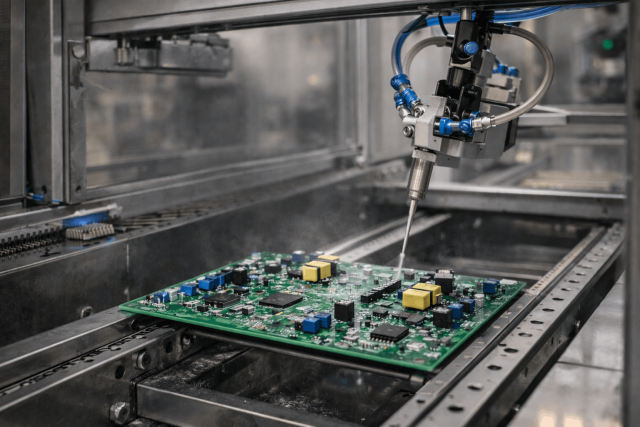
Grounding performance depends not only on design but also PCB manufacturing quality.
Important factors include:
PCB Stack-Up Control
A proper stack-up ensures:
- Stable impedance
- Reliable reference planes
- Better electrical performance
Copper Distribution
Balanced copper distribution helps prevent:
- PCB warpage
- Manufacturing variation
Via Reliability
Reliable plated vias ensure stable electrical connections between ground layers.
Manufacturing control is essential for maintaining long-term grounding performance.
Conclusion
Grounding is a critical factor in electronic design that directly affects signal integrity, EMI performance, power stability, and product reliability.
From single-point grounding and ground plane design to RF grounding and high-current power grounding, selecting the correct technique requires understanding circuit characteristics and operating conditions.
With increasing demand for high-speed communication, compact designs, and reliable electronic systems, optimized grounding strategies have become essential throughout PCB development.
By applying proper grounding techniques during the design stage, engineers can reduce noise issues, improve system performance, and achieve more reliable electronic products.
