
Healthcare PCB isolation for a patient monitor starts with a system boundary, not a board outline. A monitor can meet its functional targets in a bench setup and still fail a board-level review when the patient-connected signal domain, digital processor, and power conversion are treated as one undifferentiated ground system. On a Healthcare PCB, isolation is a system boundary that shapes the schematic, stackup, connector placement, power topology, and verification plan. The reference design notes from Texas Instruments describe several isolated power and data options for a patient-monitor module; those examples are architecture references, not universal requirements for every device.
Define the Healthcare PCB patient-side boundary before placing components
Start with the actual product architecture: which sensors or electrodes connect to the patient, which circuits sit on the applied-part side, where data is processed, and how power enters the enclosure. Draw a boundary diagram that includes analog inputs, shields, connector shells, programming headers, debug ports, charging paths, and cables. Any conductor that can cross between domains needs an explicit treatment in the system design. A Healthcare PCB review should use the device owner’s approved safety architecture and risk analysis; a PCB layout by itself cannot establish medical-device compliance.
Keep the isolated front end and the host domain visible as separate layout zones from the first floorplan. Place patient-side protection and acquisition parts near the patient connector when that suits the circuit, while locating noisy digital clocks and switching nodes outside the sensitive input corridor. Reserve room for the transformer or isolated power module, digital isolation components, barrier keepout, and the mechanical structures needed to maintain the intended separation. This multilayer PCB stackup must make the barrier inspectable across every copper layer, not only on the top-side drawing.
For a Healthcare PCB patient monitor, the selected isolation topology must match the approved system architecture and real operating modes.
Choose an isolated power topology from system needs
TI’s patient-monitor application report compares conventional and primary-side-regulated flyback options, open- or closed-loop push-pull designs, and integrated isolated power/data approaches. Each changes the board in a different way: transformer footprint and pinout, switching-current loop, feedback route, output filtering, thermal distribution, and component height. The report’s example voltages and power levels describe its reference use case only. Select a topology from the real input range, output rails, load transients, acoustic constraints, available area, and approved isolation requirements rather than lifting a reference value into a new design. A isolated power prototype assembly can check mechanical fit and integration with the planned rails.
For a flyback implementation, keep the high-di/dt primary loop compact and keep its return local to the primary switch and transformer pins. Route the secondary loop independently and place rectification and output capacitors close to their current paths. For push-pull, review switch-node balance, transformer drive symmetry, and the currents in both primary branches. In either case, the control or feedback path must respect the isolation architecture. A deliberate PCB prototype build can help evaluate fit, thermal rise, and electrical behavior, but a prototype result only applies to its documented configuration.
Plan the patient-side rail budget together with the front-end noise budget. A converter on a Healthcare PCB can satisfy average load demand yet disturb acquisition through ripple, common-mode capacitance, or a poorly returned switching current. Consider quiet intervals only when the device architecture and firmware can support them; do not assume that a filter or shield fixes an uncontrolled current loop. Check load step, startup, brownout, battery state, charging condition, and radio or display activity in the same verification plan.
A Healthcare PCB layout review should make every part of that boundary visible in the placement and layer views.
Translate the isolation barrier into PCB geometry
Make a continuous barrier region in the placement and every copper-layer view. Define which layers contain primary copper, secondary copper, or no copper, and show where the separation changes near connectors, board edges, mounting hardware, slots, and test fixtures. Do not route planes, copper pours, stitching vias, shield traces, or thermal reliefs across the boundary unless the approved design specifically permits them. If a slot is used, include its finished dimensions, tolerances, edge quality, and fabrication notes in the release package. Capture those details in the PCB fabrication review before files are frozen.
Creepage and clearance depend on the end-product standard, insulation category, working voltage, pollution degree, material group, altitude, coating assumptions, and other system conditions. There is no single safe spacing that can be copied across all patient-monitor boards. Have the responsible electrical-safety engineer set the required geometry, then make the CAD rules, fabrication drawing, and inspection checklist agree. A focused PCB design-for-manufacturing review should check that slots, mask openings, copper setbacks, and board-edge clearances remain manufacturable after routing and panelization.
Review connector shields and chassis contacts separately from signal returns. A metal shell may be bonded to chassis, to a designated shield region, or handled through a designed network; its role must be explicit. Keep mounting screws, conductive spacers, heatsinks, and test clips out of the isolation path unless their relation to the barrier has been assessed. When the board uses separate reference planes, describe each plane’s boundaries and the allowed bridge points in the stackup and assembly notes.
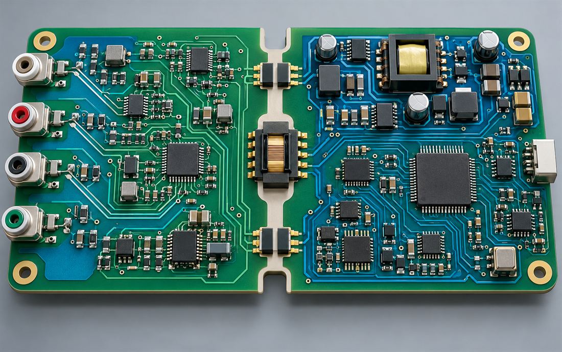
Control data and clock crossings
Every signal crossing between patient-side acquisition and host processing needs an intentional isolation path, including serial data, clocks, control lines, lead-off status, and fault indicators. Check the isolator’s channel direction, default state, timing, edge rate, and supply arrangement against the selected AFE and processor. Avoid an unplanned copper bypass through a cable shield, programming header, debug connector, or common test fixture. A schematic checklist should be paired with a net-by-net layout inspection so that no signal crossing disappears between block diagrams and routed Gerbers. A PCB engineering design review can reconcile the schematic boundary map with the manufacturing data.
Place bypass capacitors at each isolator supply pin with a short return to that domain’s local reference. Keep fast digital edges away from high-impedance analog inputs and avoid routing clocks parallel to sensor traces over long distances. If the design has multiple isolated channels, map their data, power, and reference domains individually; similar-looking symbols do not guarantee that the physical barriers align. The manufacturing drawings should identify components that bridge the physical boundary and include polarity, orientation, and inspection references.
Prototype review should include the actual power source, cable set, enclosure, and communication state. A Healthcare PCB build with a bench supply or short cable can hide coupling that appears after the product is assembled. Ask the team to record the firmware build, board revision, sensor connection, and radio or display activity for every observation. This turns an intermittent data or noise complaint into a comparison of known configurations instead of a series of unrelated component changes.
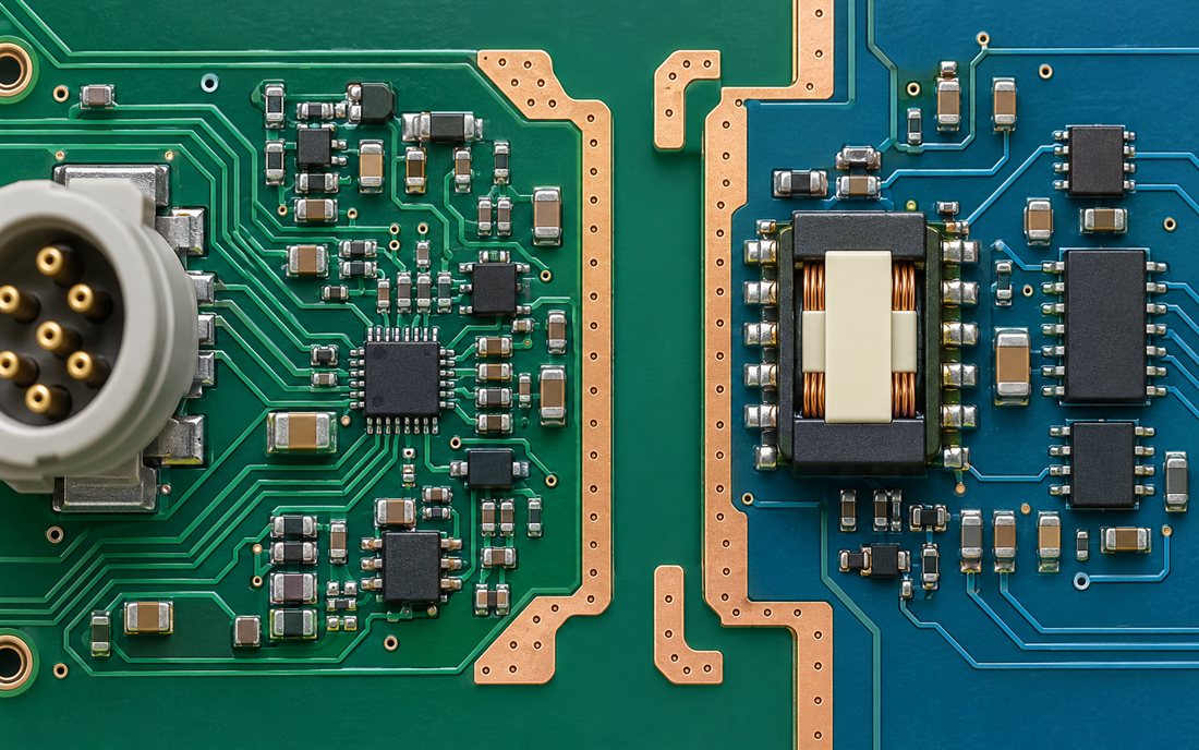
Verify the assembled boundary under defined conditions
The device manufacturer should define applicable safety and EMC tests, acceptance limits, operating modes, and representative use environments. FDA EMC guidance discusses device-level emissions and immunity assessment; it does not certify a bare PCB or replace the product-specific regulatory plan. At board level, prepare repeatable checks for power-up, load steps, conducted noise, acquisition stability, barrier inspection, isolation components, and communications faults. Identify which checks are engineering characterization and which belong to formal compliance testing. Record the sequence in a PCBA prototype test plan tied to the exact revision.
Use documented fixtures and probes. Record test-point loading, grounding, cable routing, enclosure panels, source impedance, and instrument bandwidth so two builds can be compared fairly. Keep each PCB prototype test fixture configuration under the same revision record. Verify relevant supply rails at the AFE and host loads, not only at the connector. Check that transient current from a display, radio, or motorized accessory does not disturb the analog domain under the chosen architecture. If a result changes after a component substitution or layout revision, preserve the original setup and rerun the same checks before drawing a conclusion.
Close the safety review with the responsible product team. PCB spacing, isolator datasheets, and a passing engineering check are supporting evidence; together they are not a blanket claim that the complete device satisfies a standard. Keep the Healthcare PCB test record tied to the exact schematic, layout, BOM, firmware, enclosure, and cable revision so later verification can identify what changed.
Release a fabricable, traceable board package
Issue one controlled package containing the stackup, copper weights, finished board outline, fabrication files, drill data, slot details, assembly drawing, BOM, approved alternates, and barrier-specific notes. State which dimensions are critical to the isolation architecture and how they should be inspected. For an isolated transformer footprint, include pin-one orientation and the keepout around both winding groups. For a digital isolator, show its orientation and the copper separation beneath and beside the package according to the selected design rules.
Ask manufacturing engineering to review panel rails, coupons, test access, solder-mask registration, component clearances, and assembly sequence before release. Specify any cleaning, coating, or inspection requirements only when they are part of the validated product process. The SMT PCB assembly process should preserve the physical boundary and component orientation in the actual build; AOI or electrical test cannot replace a design review of copper spacing.
For a new revision, track deviations and approved changes in the same release record. A supplier question about a slot, laminate, transformer, isolator, or test point should return to the responsible design owner before manufacturing files are altered. A prototype assembly review can reveal fit and access issues, while the released production package remains the authority for subsequent lots.
In short, a patient-monitor isolation boundary begins with the system architecture and becomes real through placement, routing, fabrication notes, assembly controls, and verification. A reliable Healthcare PCB review ties those decisions to one configuration and leaves safety and compliance conclusions to the qualified product team.
Sources: Texas Instruments, “Topology Selection for Isolated Power Supplies in Patient Monitor” (SLOA285A), for architecture options and patient-monitor examples; U.S. FDA, “Electromagnetic Compatibility (EMC) of Medical Devices” (June 2022), for device-level EMC assessment context; Analog Devices pulse-oximeter technical article, for an example of sensitive optical and analog signal paths. Reference design details are case-specific. No customer measurement, KKPCB test result, or certification claim is represented.

