
A low-noise ultrasound receiver can be routed correctly and still lose performance after assembly. The failure is often introduced by an ordinary production step: an aggressive wash reaches a probe contact, ionic residue remains beside a high-impedance input, or conformal coating creeps into a connector keep-out. These are not cosmetic issues. They alter leakage, parasitic capacitance, surface insulation, and the return-current environment that the analog front end depends on. This guide treats the Ultrasound PCB cleaning and coating decision as part of the electrical release.
The objective is not to prescribe one chemistry for every instrument. It is to give engineers and project managers a controlled method for protecting the receive path while keeping the board manufacturable, inspectable, and serviceable. The examples are engineering controls and design targets, not claims of a customer test. This Ultrasound PCB cleaning decision should be reviewed with the receive-chain owner before the assembly traveler is frozen.
- Map the contamination risk before layout freeze
- Design cleaning and drying into the release
- Keep coating away from sensitive boundaries
- Make cleanliness evidence inspectable
- Close the production handoff
Map the contamination risk before layout freeze
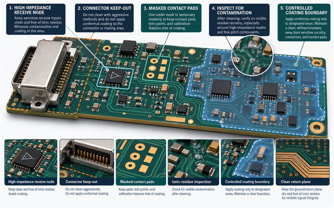
The first question is where a small amount of residue can create a large electrical change. The Ultrasound PCB receive input, bias network, probe connector, and calibration node should be marked as different risk classes. A high-impedance input can be affected by a film that would be irrelevant on a power plane. A connector cavity can trap wash fluid and release it slowly. A calibration pad can become unreadable when coating overlaps its edge.
Create a contamination map next to the floorplan. Mark the high-impedance receive nodes, exposed contacts, acoustic or probe connector, test pads, vents, and areas that will receive coating. Then connect each region to an owner: layout, assembly, cleaning, inspection, or service. This turns a vague “keep it clean” note into a practical Ultrasound PCB release rule. It turns a vague “keep it clean” note into a practical PCB design constraint.
Separate electrical sensitivity from mechanical exposure
The receive node may be electrically sensitive but physically protected under a shield. The connector may be electrically robust but mechanically exposed to wipes, handling, and repeated mating. Do not assign the same process rule to both. Use the PCB materials review to confirm the laminate, solder mask, surface finish, and coating compatibility before selecting a wash process.
A useful early table has four columns: region, contamination consequence, allowed process, and verification method. For example, the receive input may require a no-residue inspection and a defined dry condition; the connector may require masking and a visual contact check; the board edge may require a surface-finish and wear review. The exact process window belongs in the manufacturing traveler after the chemistry and component vendors are confirmed.
Design cleaning and drying into the release
Cleaning is a process, not a single machine setting. On an Ultrasound PCB, the receive path makes small process residues more consequential than they would be on a low-impedance power board. Water quality, chemistry concentration, spray direction, dwell time, rinse quality, and drying all affect what remains on the board. A supplier may be able to wash an ordinary PCB manufacturing panel successfully, while an Ultrasound PCB connector cavity still retains fluid while a dense ultrasound board still retains fluid under a connector shell or between a shield and a high-impedance component.
Define the board orientation and shadow zones in the assembly traveler. If a connector blocks spray access, specify a secondary inspection or a fixture rotation. If an acoustic shield or bracket creates a pocket, show how the pocket is drained and dried. Avoid relying on compressed air alone when it can drive fluid deeper into a cavity. The cleaning owner should provide the approved chemistry, concentration, temperature, and drying method; the electrical owner should confirm that the method does not create a new leakage or dielectric issue.
Protect contacts and calibration features
Mask connector contacts, probe mating areas, test pads, and calibration features before any process that could deposit coating or leave a film. The mask must be compatible with the selected chemistry and must not tear into a fine-pitch pad array. Record the mask removal step, because a clean board can still fail when adhesive residue remains at the contact edge. This is especially important on an Ultrasound PCB where the same edge may sit beside a sensitive receive trace.
For a PCB assembly line, show the mask boundary on the assembly drawing rather than on a private process note. The operator should be able to see which areas are protected and which are intentionally exposed. A simple color overlay or keyed drawing reduces rework caused by ambiguous “connector keep-out” language.
Drying is equally important. Require a board temperature and time range suitable for the laminate, components, adhesives, and connector. If the board is held before coating, define the maximum exposure time and storage condition. Project managers should treat this as a queue-control problem: a clean but wet board waiting overnight is not the same as a clean, dry board released to coating. The Ultrasound PCB traveler should make that state visible to quality and assembly.
Keep coating away from sensitive boundaries
Conformal coating can improve environmental protection, but it should not be used as a substitute for a sound layout or cleaning process. On an Ultrasound PCB, coating changes surface capacitance and can alter the field around high-impedance inputs, guard traces, and fast connector launches. The coating boundary for an Ultrasound PCB therefore belongs in the electrical drawing and the PCB fabrication or assembly notes. For an Ultrasound PCB, this boundary is an electrical control as well as a process marking.
Define three zones: coated, uncoated, and conditionally coated. The uncoated zone should include probe contacts, mating surfaces, calibration pads, vent openings, and any feature that must be inspected or reworked. The conditionally coated zone may include a receive network or shield edge if the component vendor and reliability owner approve the material and thickness. Do not let the applicator infer the boundary from component outlines alone; solder mask, test pads, and the connector shell can extend beyond the component body.
Review thickness and edge control
A target coating thickness is meaningful only when the application method and inspection method are defined. Spray, selective dispense, and dip processes create different edge profiles and shadow zones. Specify the keep-out offset from a high-impedance pad, connector contact, and switch node. Then show how the operator verifies the edge: optical inspection, a witness coupon, a fluorescent additive, or another approved method.
The controlled-impedance PCB conversation should also include coating assumptions when the material sits near a fast edge or a connector launch. If the coating is removed for service, define the repair method so a field touch-up does not leave a conductive or capacitive island. Where the exact electrical effect is uncertain, state the design target and schedule a board-level confirmation rather than inventing a measured value.
Make cleanliness evidence inspectable
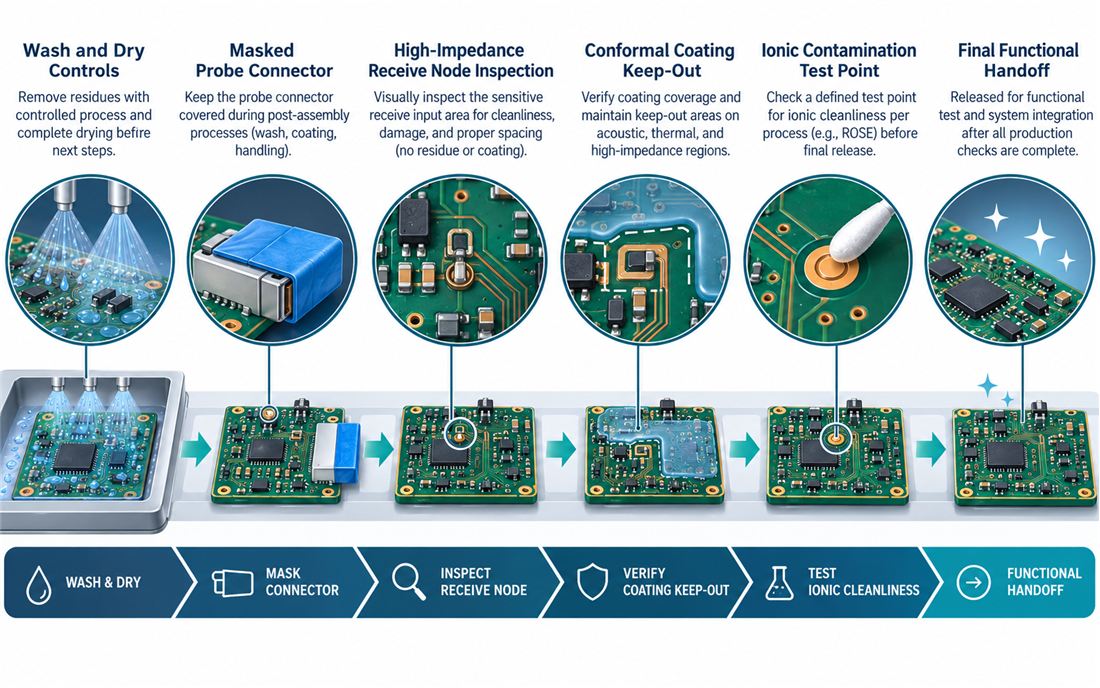
Inspection must answer a specific question. Visual inspection can show particles, bridging, coating creep, or an unmasked contact, but it cannot prove every ionic or moisture risk. Define the inspection method for each risk class. A high-impedance receive region may require magnification and a no-residue criterion. A connector may need contact and cavity inspection. A coating boundary may need a witness feature or a fluorescent check. The PCB testing plan should list the method, sample size, owner, and release disposition.
Do not label a conceptual cleanliness illustration as a test result. The second figure below shows a possible release flow; it does not represent a KKPCB customer measurement. Actual ionic cleanliness, insulation resistance, or functional data should be recorded only with the approved fixture and method.
Connect inspection to rework limits
A board can pass inspection and still be difficult to repair if the rework boundary is undefined. State whether a contaminated receive node may be cleaned locally, whether coating can be removed, and how the board is re-inspected after rework. For a serviceable PCBA, identify the safe probe point and the mechanical support needed to avoid stressing a connector or fine-pitch package.
Use the PCB prototype to validate the inspection sequence, not just to demonstrate that the board powers up. The prototype should use the intended mask, connector cover, coating boundary, and documentation. Otherwise, production may discover that a feature is technically inspectable but inaccessible with the real fixture.
Close the production handoff
The final release package should carry one consistent map of cleaning, masking, coating, inspection, and rework. Include the approved material or chemistry names, the regions they apply to, the drying and hold conditions, the connector protection method, and the acceptance evidence. A multilayer PCB drawing should show the high-impedance node and return plane in the same revision package as the coating drawing; otherwise a late layer or pad change can move the electrical boundary without triggering a process review.
Change control is critical when a component, connector, or coating supplier changes. Re-check pad spacing, keep-out, cleaning compatibility, cure temperature, inspection access, and repair instructions. A new connector may require a new mask. A new coating may change the guarded node’s capacitance. A new wash chemistry may change the acceptable drying time. The PCB manufacturing review should record the impact and the responsible owner before the change is released.
A concise first-panel checklist is:
- Receive nodes, probe contacts, calibration pads, and coating zones are marked on the same drawing.
- Cleaning chemistry, rinse, drying, and maximum hold time are approved by the process owner.
- Connector and contact masks are visible to the assembly operator and removable without residue.
- Coating boundaries, thickness target, and inspection method are defined for every sensitive region.
- Rework, service, and post-rework inspection limits are written before the first panel.
When these controls are connected, the Ultrasound PCB release is easier to explain to engineering, manufacturing, quality, and procurement. The board is not merely clean on the day it leaves the washer; its sensitive nodes, connector contacts, coating edges, and evidence package remain controlled through assembly and service.
Sources: selected component, connector, coating, cleaning, and probe data sheets; approved laminate, solder-mask, surface-finish, and fabrication data; assembly process instructions; and engineering guidance from Analog Devices, Qorvo, Würth Elektronik, and relevant medical/RF PCB references. Values and checks in this article are design targets or engineering methods, not customer measurement claims.
