
Table of Contents
Manufacturers often discover a traceability gap only after a field return: the serial number is known, but the team cannot prove which fabrication lot, assembly process, firmware revision, or functional test was associated with that unit. A Smart Factory PCB should make that chain possible without turning the board into a barcode experiment. The Smart Factory PCB needs identifiable revision marks, stable test access, repeatable programming points, and a manufacturing package that preserves the relationship between physical features and digital records.
This production-focused article addresses the project manager who must release a high-mix controller across several suppliers. The goal is not to claim a particular customer result. It is to show how a Smart Factory PCB can carry enough evidence for incoming inspection, assembly, functional test, and service analysis without adding unplanned rework.
Why traceability starts in the PCB release
Smart Factory PCB traceability is frequently treated as an MES or ERP function, while the physical board is left with a generic part number and a small date code. That separation creates ambiguity. If the serial label is placed on a replaceable cover, the label can become detached from the board. If a revision is hidden under a connector, an inspector may record the wrong variant. The first design review for a Smart Factory PCB should therefore define a visible board identifier, a machine-readable mark, and a rule for when that mark is created.
Choose the identifier location for the Smart Factory PCB with the PCB design team and the inspection team together. Reserve a clear silkscreen area, keep it away from solder-mask openings and fiducials, and define a contrast requirement that the camera can read after cleaning. When the board is conformally coated, decide whether the code is printed before coating, laser-marked after coating, or stored only in the assembly record. That decision changes the drawing, the process route, and the service instruction.
Design test access into the layout
A traceability record for a Smart Factory PCB is only useful if the production test can prove that the physical board is the board described by the record. Give the functional fixture access to power rails, reset, communication, safety interlocks, and the key analog or sensor nodes. Boundary-scan pads may be appropriate for dense digital nets, while dedicated test points are more reliable for a power-tree check or a connector-loopback test. A PCB manufacturing drawing should identify keep-outs, probe-side access, pad finish, and the acceptance method for each point.
Do not scatter test points wherever there is unused copper. Group them by fixture function and keep their datum consistent across panel designs. A test point that is electrically correct but hidden below a tall connector becomes a manual touch-up operation. For boards with high-speed interfaces, the test strategy must also protect signal integrity: probe stubs, unused via branches, or an improvised coax adapter can change the very net being validated.
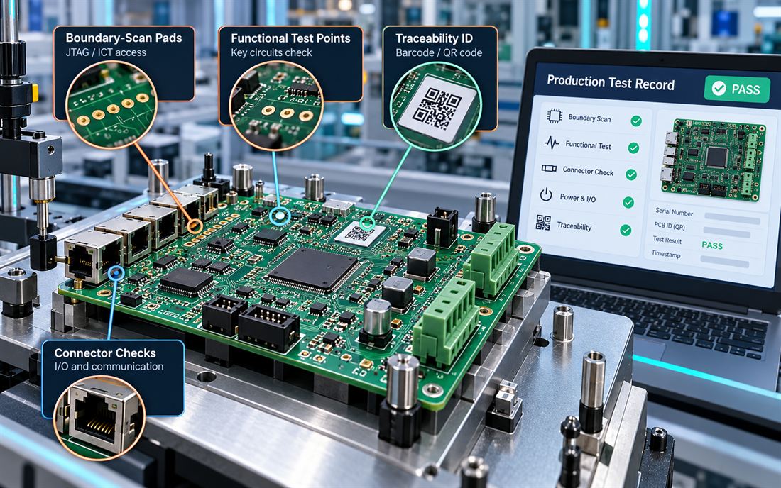
Make the test record unambiguous
Each Smart Factory PCB test step should write a result against a unique board or panel identifier, not only against a work order. Store the firmware version, fixture revision, operator or station ID, and the disposition of a failed test. If a repair is allowed, record the replaced component and the retest result rather than overwriting the original failure. This gives engineering a way to separate a design weakness from an assembly escape.
Connect panel data to assembly evidence
Panelization is where a Smart Factory PCB many traceability schemes lose their physical anchor. A panel ID may be scanned at fabrication, but individual boards can be mixed during depanelization unless the board-level mark and the panel map agree. Use global fiducials for the panel and local fiducials for each board where the assembly process needs them. Include a panel drawing that identifies breakaway features, tooling holes, coupon locations, and the location from which a board-level code remains readable.
The PCB materials choice affects this workflow when surface finish, coating, or a dark solder mask changes code contrast. Record the released laminate, copper construction, and finish in the same revision package. A second supplier should not be allowed to substitute a material or PCB finish that makes optical identification unreliable simply because the electrical netlist still passes.
During PCB assembly, link AOI, X-ray, programming, and functional-test results to the same identifier. The exact station sequence can vary, but the data model should retain the order. This is particularly important for a board that has a calibration constant written during final test: the constant must remain tied to the board serial number after rework or a firmware update.
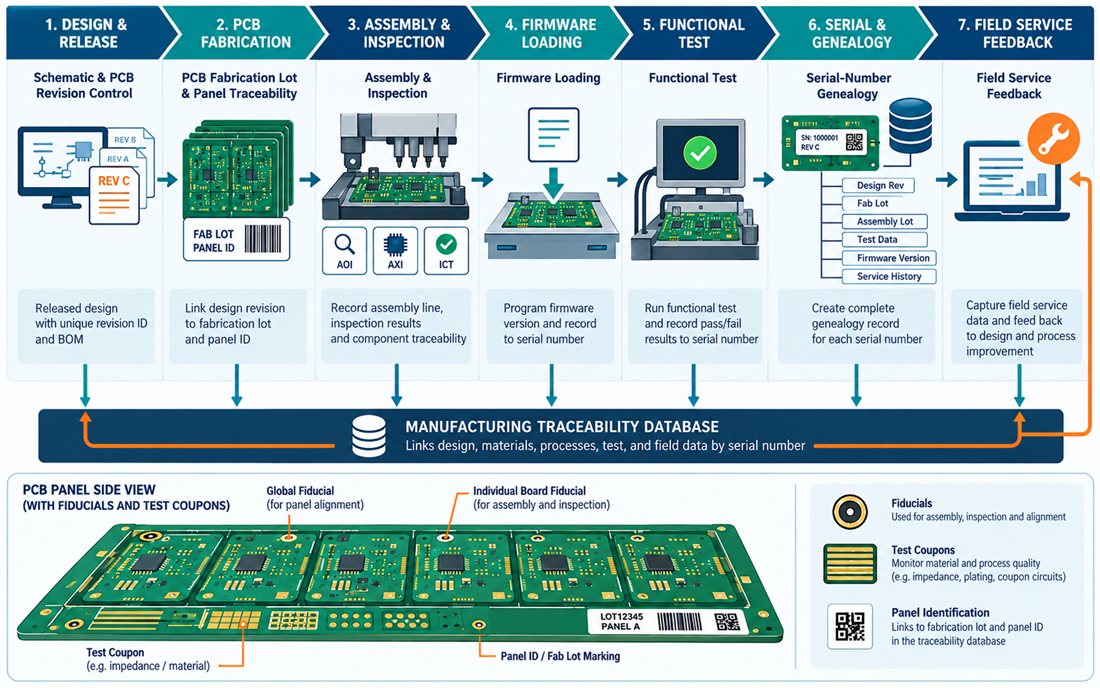
Close the service loop
Field service for a Smart Factory PCB needs a concise record, not a dump of every station log. Expose the board revision, manufacturing identifier, firmware version, and a small set of diagnostic values through a service connector or protected software screen. A robust PCB fabrication package makes those identifiers durable: use an agreed marking process, define allowable placement variation, and keep the marking away from areas that are removed during depanelization.
When a failure trend appears, compare the field population by fabrication lot, assembly line, component date code, and firmware revision. That comparison is only meaningful when the design record is stable. The PCB prototyping build should therefore exercise the complete scan-to-service path, including a deliberately rejected board and a repaired board. Do not wait until volume production to discover that a repaired unit receives a new serial record instead of a traceable revision.
Five release gates
Before a Smart Factory PCB enters volume production, use five practical gates. First, confirm that the board-level identifier survives the planned finish, coating, cleaning, and service handling. Second, prove that every required test point can be reached by the fixture without unsafe probing. Third, link the panel map, assembly record, firmware load, and functional result to one identifier. Fourth, test the rework path and preserve the original failure history. Fifth, freeze the released PCB design, PCB production, and test-fixture revisions together.
These Smart Factory PCB gates also protect sourcing. A qualified assembly line should receive the same acceptance language as the fabricator, while a future controlled-return layout change must trigger a review of test pads and identification marks. When the project grows from a pilot to multiple lines, that discipline prevents a low-cost label or fixture shortcut from erasing the evidence needed to improve the next release.
Sources: IPC traceability and assembly-process guidance, manufacturer data sheets for laminate and finish compatibility, Analog Devices material on production test and mixed-signal grounding, Würth and Qorvo engineering references for controlled-return layouts, and KKPCB capability pages for design, materials, fabrication, and assembly planning. Process values in this article are release targets and engineering practices, not customer test results.
