
A smart factory controller can lose production time without ever dropping a visible network link. A connector shield is bonded through a long path, a time-reference trace crosses a noisy converter, or the enclosure forces an unexpected return current through the Ethernet PHY. A Smart Factory PCB that carries deterministic industrial Ethernet must treat magnetics, differential pairs, clock distribution, isolated power, and chassis bonding as one physical system.
A Smart Factory PCB review should include the enclosure, cable, switch, power, and timing assumptions before layout release.
The project problem is usually discovered during system integration: the link establishes on the bench, but traffic becomes less predictable when a second node, long shielded cable, or machine drive is added. This article gives an engineering release method for edge controllers and gateway boards without claiming a customer measurement or compliance result.
- Place the Ethernet entry and shield datum before routing the processor.
- Keep differential pairs, clock paths, and power returns physically explainable.
- Separate noisy conversion current from the quiet PHY and processor zones.
- Verify the complete node, cable, switch, and enclosure—not only a bare board.
Table of contents
For a Smart Factory PCB, the Ethernet entry is the physical boundary between the machine cable and the controlled board reference.
Start with the Ethernet entry and chassis datum
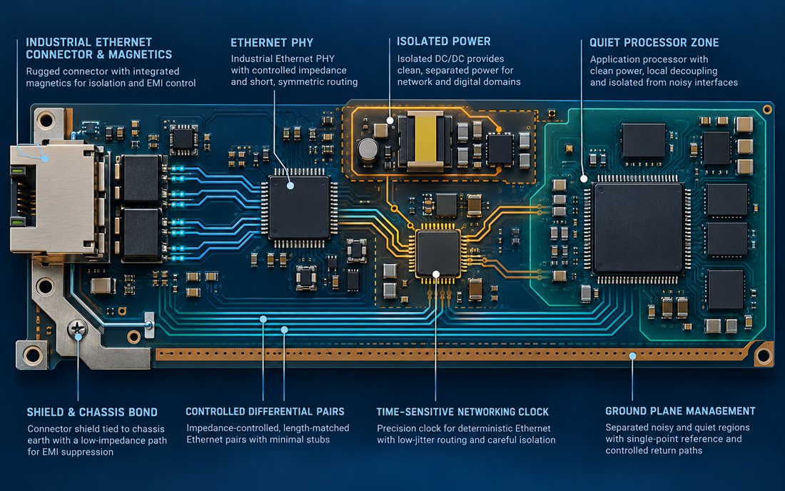
The first layout review of a Smart Factory PCB should mark the connector shield, magnetics, PHY, and the path to chassis or protective earth. Place the magnetics close to the connector and keep the shield bond short and wide. If the enclosure uses a painted panel, define the conductive hardware or contact area that makes the bond; do not assume the mounting screw creates a repeatable RF connection.
The PCB materials stack controls the geometry available for a controlled Ethernet pair. Do not copy an impedance value from a reference design without checking actual dielectric thickness, copper roughness, finished copper, and fabrication tolerance. The supplier and designer should agree which geometry is controlled and which value is a design target.
Keep pair transitions and return vias deliberate
Route each differential pair with a continuous reference and avoid crossing a plane split created for an isolated supply. When a pair changes layers, provide a nearby return path so the transition does not force current around a cutout. A high-frequency PCB review habit is appropriate because edge rates, connector discontinuities, and shield currents can matter even when the nominal network speed is not extreme.
Keep stubs, test pads, and vias out of the launch unless they are part of the controlled design. A connector alternate can move the pin field or shield contact, so the PCB manufacturing package should identify the approved footprint, stack, and any controlled pair requirement.
A Smart Factory PCB preserves deterministic behavior when time and data paths are reviewed as separate but coordinated interfaces.
Treat time and data paths as separate critical interfaces
A deterministic network adds a timing problem to the ordinary data-routing problem. The oscillator, synchronization device, PHY reference, and processor clock need a quiet supply and a return path that does not share the highest-current converter loop. For a Smart Factory PCB, show the clock path and its guard region in the layout review so a late fan-out change does not pass through the magnetics or power zone.
Keep processor memory and high-speed expansion buses away from the Ethernet entry when possible. If the architecture requires a crossover, define the plane and return strategy instead of simply adding copper. The fabrication release should show layer references, drill transitions, and any back-drill or via treatment that the signal path actually needs.
Make isolation and reference coupling visible
Many factory nodes include an isolated port, isolated power, or a chassis capacitor network. Draw the coupling points and their intended current direction. A small capacitor to chassis can be useful for common-mode control, but its placement and return inductance determine whether it helps or creates a new current loop. The PCB assembly traveler should identify polarity, package, and any no-clean or cleaning requirement for those interface parts.
Do not use the enclosure as an undefined signal reference. If the board is mounted on a metal carrier, show whether the carrier is chassis, shield, or mechanical only. This prevents system integration from changing the network return without a board revision.
The Smart Factory PCB power architecture must keep converter current away from the PHY, clock, and processor reference.
Keep power conversion from modulating the network zone
Edge controllers often combine an input converter, isolated power, Ethernet magnetics, processor power, and I/O. Give each converter a compact hot loop and keep its switching node away from the PHY and clock. The Smart Factory PCB should include thermal vias, copper spreading, and the ability to inspect or probe the power rails after the board is assembled.
Thermal gradients can change oscillator behavior, PHY margin, and connector reliability. Locate hot inductors and switching devices where the enclosure can remove heat without directing it into the clock or magnetics. If a heat spreader or shield can touches the board, document its electrical relationship before the surface finish and coating are selected.
Reserve service access without adding uncontrolled stubs
Test points are needed for power and firmware bring-up, but a convenient pad on a differential pair can add a stub. Use guarded, documented access points and keep them outside the controlled launch. A prototype PCB should be tested in the intended enclosure so service access, cable bend, and thermal flow are not inferred from a desk setup.
A Smart Factory PCB is not system-ready until its cable, switch, enclosure, clock, and power conditions are validated together.
Validate deterministic behavior as a system
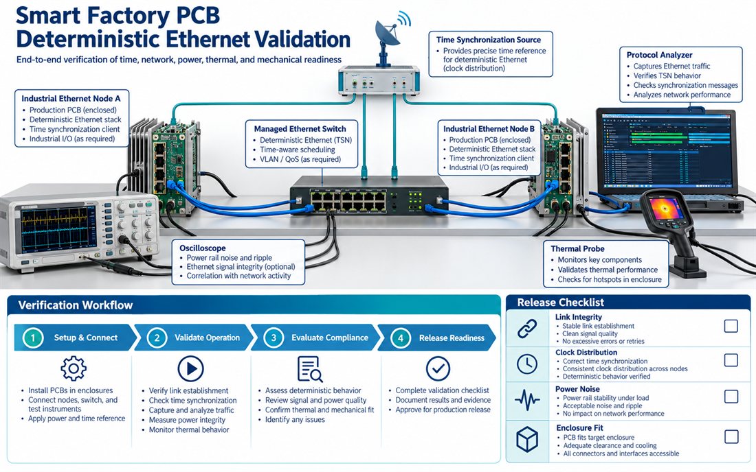
A network validation fixture should include at least two representative nodes, the intended switch or traffic source, shielded cable, time-reference source, and the power conditions expected in the machine. Observe link establishment, synchronization behavior, error handling, power noise, and enclosure temperature as separate questions. The second illustration is a conceptual workflow; it is not a claim of measured customer performance.
Map every observation to a release action
Record the board revision, PHY configuration, cable type, switch configuration, and fixture wiring. The assembly fixture should carry the same identifiers as the firmware and network test script. If an issue appears only with a long cable or a metal enclosure, record the condition instead of reducing it to a generic pass or fail.
| Release item | Question | Evidence |
|---|---|---|
| Ethernet launch | Are shield, magnetics, pair geometry, and return path consistent? | Layout review and connector inspection |
| Clock path | Does synchronization remain isolated from converter noise? | Clock power review and system fixture record |
| Power/thermal | Can the enclosure remove heat without moving PHY or oscillator behavior? | Design target and thermal inspection |
| Configuration | Do hardware, switch, and firmware identifiers match? | Controlled release matrix |
Freeze the node contract before production purchasing
The Smart Factory PCB purchase release should preserve the approved magnetics, connector, clock, and system-test assumptions.
Before releasing the next lot of a Smart Factory PCB, freeze the connector, magnetics, pair geometry, clock source, shield rule, power modules, and system test setup. A substitute PHY or connector can change pin mapping, thermal load, and common-mode behavior even when the headline data rate is unchanged. Attach the approved PCB manufacturing package and material assumptions to the purchase release.
A Smart Factory PCB production node is ready for deterministic traffic when the board, cable, switch, enclosure, power, and configuration records tell the same story. A controlled pilot node is the practical checkpoint before a production line is committed.
The Smart Factory PCB handoff is strongest when network, power, thermal, and configuration evidence agree.
Sources: Analog Devices Ethernet, clock, and signal-integrity application guidance; Würth Elektronik connector, magnetics, grounding, and assembly notes; Qorvo interface references; Ethernet PHY, switch, enclosure, and PCB material supplier application data. The diagrams are original conceptual engineering graphics and do not represent a customer measurement or qualification report.
