
Machine-vision systems turn a factory camera into a high-speed mixed-signal problem. The image sensor, illumination driver, serializer, FPGA, memory, and processor share an enclosure, while a cable or connector crosses the same boundary as a noisy LED supply. A Smart Factory PCB for image acquisition must preserve timing and signal margin without letting illumination current or converter noise pollute the analog front end.
A Smart Factory PCB vision review should include sensor, light, cable, enclosure, clock, and processor conditions before image quality is judged.
Projects often discover the problem when image quality changes with lighting intensity, cable length, or processor load. This article provides a practical way to zone the board, control the reference clock, protect the high-speed link, and validate the complete camera node. The diagrams are conceptual engineering aids, not customer measurements.
- Separate sensor, serializer, processor, illumination, and power zones.
- Give the reference clock and analog front end a quiet return.
- Control high-speed launches, connector shielding, and enclosure coupling.
- Test image, timing, power, thermal, and mechanical behavior together.
Table of contents
For a Smart Factory PCB camera node, the image path is the placement spine for the entire board.
Zone the vision board around the image path
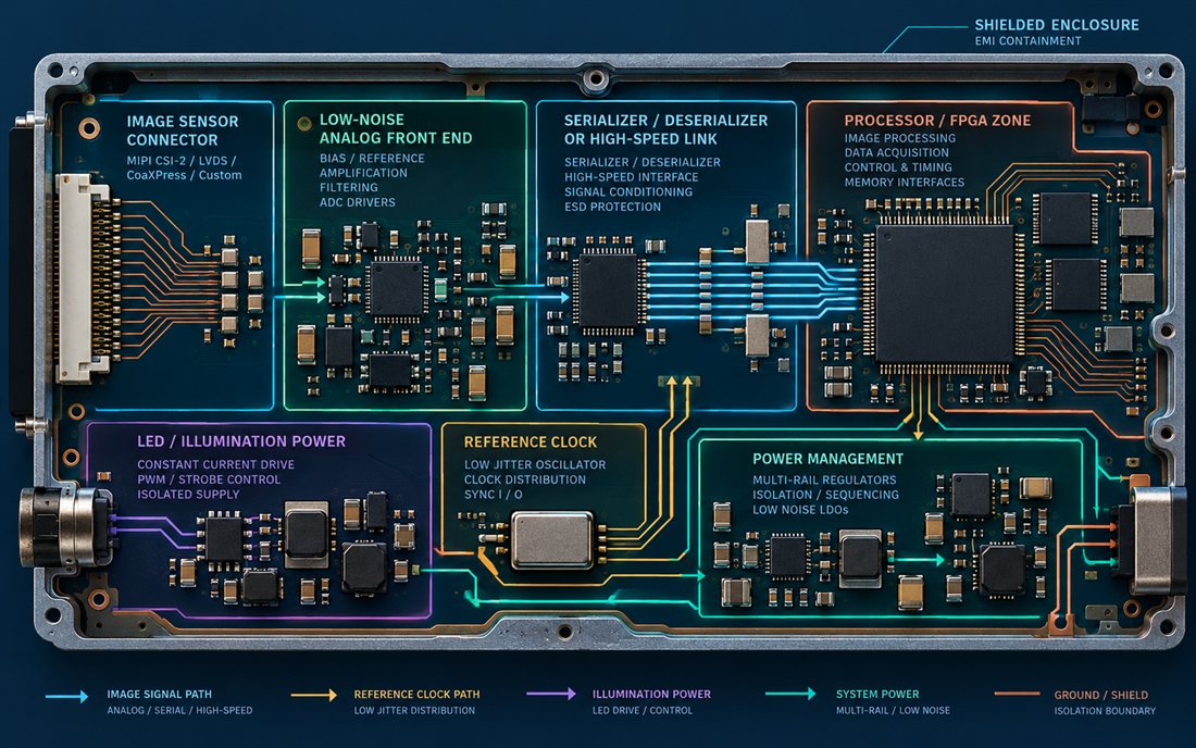
The first placement review of a Smart Factory PCB should start at the sensor connector and follow the image data to the serializer, FPGA, memory, and external link. Keep the low-noise analog front end close to the sensor and away from the LED driver and switching converter. The PCB materials stack controls the pair geometry and reference depth, so the camera interface should be planned with actual fabrication capability rather than a generic stack.
Give the image path a continuous reference and avoid crossing a plane split. If a connector or layer transition is necessary, provide a nearby return path and keep the launch symmetrical. The enclosure boundary should show where shield, chassis, and signal references meet; otherwise a camera cable can inject current into the analog region through an unplanned bracket or spring.
Keep illumination current out of the sensor reference
LED or strobe drivers create fast current edges and local heat. Give them a compact loop and a separate return to the power entry. A high-frequency PCB layout discipline helps because the current loop includes parasitic capacitance and cable coupling, not only the DC path. Use guard spacing around the sensor reference and keep the driver switch node away from the clock and analog input.
When illumination is pulsed, the power rail may move even if the average current is low. Reserve decoupling close to the driver and define how the rail is monitored during image capture. The PCB manufacturing package should identify copper regions, thermal vias, and any controlled impedance requirement that is essential to the image link.
An Industrial vision Smart Factory PCB keeps clock and image references explainable when processor activity changes.
Protect clock and image paths from processor activity
Image acquisition boards often place an FPGA or application processor beside the serializer. Memory buses, switching regulators, and processor clocks can inject broadband noise into the sensor or the reference oscillator. For a Smart Factory PCB, route the reference clock with a deliberate return and keep it away from the LED driver and converter inductor. Do not use a long shared clock route simply because the pinout is convenient.
Keep high-speed pairs short, length-matched where required, and free of stubs. When a pair changes layers, place return vias and avoid a discontinuity at the connector. The fabrication release should define the actual drill, layer, and impedance controls that the fabricator can verify, not a list of tolerances copied from an unrelated design.
Use shielding as a controlled boundary
A camera enclosure can become part of the signal path when its shield is bonded at one end and the board mounting hardware is bonded at another. Define whether the shell, connector shield, board copper, and chassis are common or intentionally separated. The PCB assembly traveler should show shield springs, conductive gaskets, and any coating keep-out around the connector or sensor window.
If a coax or high-speed cable enters the board, protect the launch from nearby power copper. A short path to chassis often reduces common-mode coupling more effectively than a longer trace to logic ground. Keep test pads off the controlled pair unless they are part of the approved measurement method.
The Smart Factory PCB power tree must separate illumination pulses, conversion current, processor load, and sensor reference.
Manage illumination, conversion, and processor power
Power architecture is a system problem on a vision node. The illumination rail may be pulsed, the processor load may change with image complexity, and the serializer may have a sensitive supply requirement. Use local filtering and a controlled power-tree reference. The Smart Factory PCB should include thermal spreading, probe access, and the ability to inspect the power components after assembly.
Thermal gradients can shift sensor dark current, oscillator behavior, and processor timing. Place hot inductors and switching devices where the enclosure can remove heat without warming the sensor or reference oscillator. If a heat spreader touches the shell, document its electrical relationship before selecting surface finish and coating.
Keep service access without creating a noise antenna
Vision boards require connector and test access, but a long probe pad on a high-speed signal can become an antenna. Use guarded power and clock test points, keep the image launch clean, and document probe direction. A controlled prototype PCB should be tested in the camera housing with the intended lens, light source, cable, and mounting hardware.
A Smart Factory PCB is production-ready only when image, timing, power, thermal, and connector behavior are validated as one node.
Validate image, timing, and power as one node
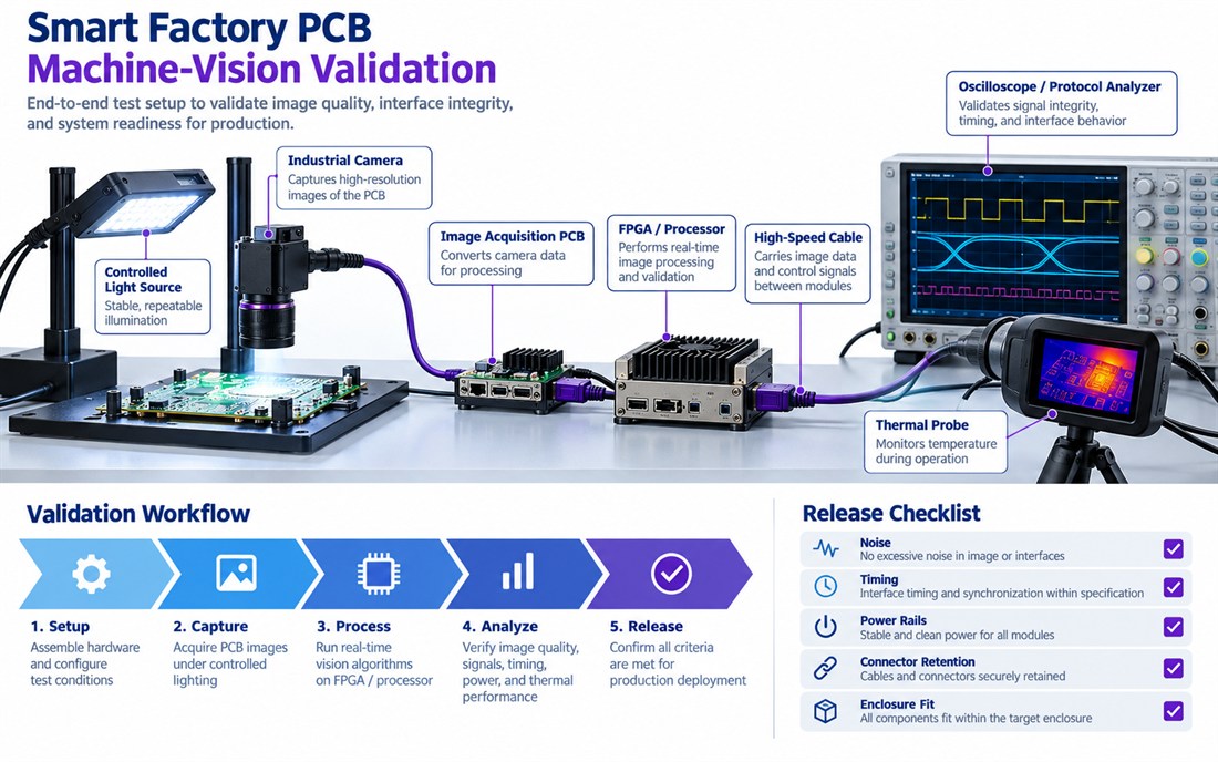
A useful validation fixture includes the camera or representative sensor, controlled light, image-acquisition board, FPGA or processor, high-speed cable, analyzer, and thermal observation. Check image stability under illumination changes, link behavior under processor load, clock synchronization, power ripple, connector retention, and enclosure fit. The second image is a conceptual workflow and does not present measured customer data.
Turn image quality observations into release gates
Record the board revision, sensor configuration, light source, cable, firmware, and fixture wiring. The assembly fixture should identify which camera and processor build it supports so an old script cannot approve a changed image path. If a noise artifact appears only with a strobe or long cable, retain the condition in the deviation record.
| Gate | Question | Evidence |
|---|---|---|
| Image path | Are sensor, serializer, connector, and pair returns continuous? | Layout review and link observation |
| Clock | Does the reference remain stable during processor and light changes? | Clock supply and timing record |
| Power | Are illumination and processor rails isolated from the analog front end? | Power-tree review and fixture setup |
| Mechanical | Do cable, connector, enclosure, and thermal interfaces remain secure? | Fit and retention check |
Freeze the camera-node contract before volume build
The Smart Factory PCB purchase release should preserve the approved sensor, serializer, clock, illumination, and test assumptions.
Before releasing the next lot of a Smart Factory PCB, freeze the sensor connector, serializer, clock, power tree, illumination driver, shielding rule, and camera configuration. A component alternate can change noise, heat, package height, or pair geometry even when the headline interface remains the same. Attach the approved PCB manufacturing package and material assumptions to the release.
A Smart Factory PCB camera node is production-ready when image path, clock, power, enclosure, and configuration evidence agree. A controlled pilot camera build is the right checkpoint before a vision line is scaled.
The Smart Factory PCB handoff is strongest when signal, power, thermal, and image evidence agree.
Sources: Analog Devices signal-chain, clock, and high-speed interface guidance; Würth Elektronik connector, grounding, and assembly notes; Qorvo interface references; camera sensor, serializer, illumination, enclosure, and PCB material supplier application data. The diagrams are original conceptual engineering graphics and do not represent a customer measurement or qualification report.
