HomeCategory

Advanced Engineering Technologies for PCB & PCBA Solutions - KKPCB

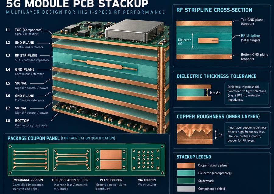
Selecting a 5G Module PCB Stackup Without Hiding the Loss Budget

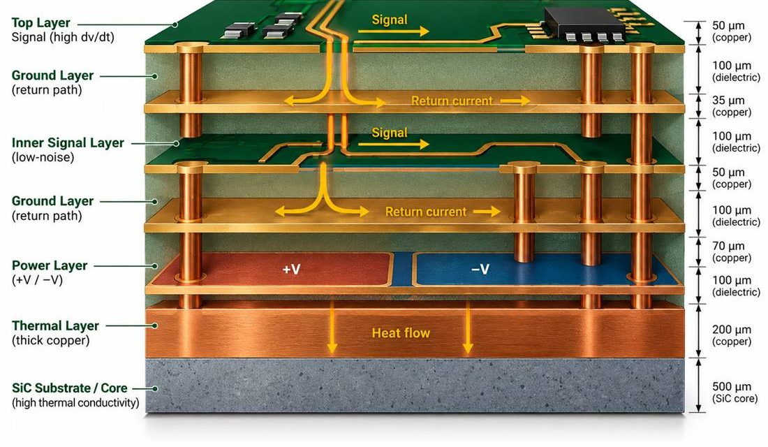
5G module PCB stackup release begins by making every electromagnetic and manufacturing assumption visible. Stackup discussions fail when the drawing lists layer names but not the electromagnetic and manufacturing assumptions behind them. In compact radio modules used in private 5G radios, fixed-wireless units, and edge gateways, the board must carry RF energy, power current, high-speed...
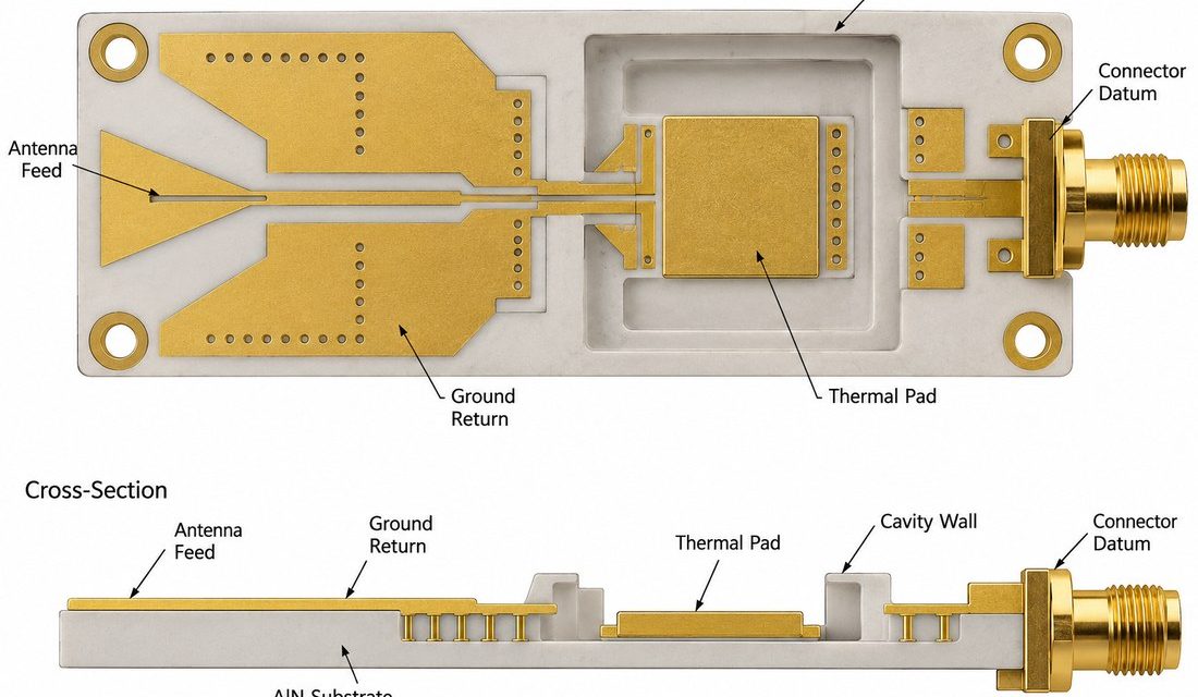
Aluminum Nitride PCB for mmWave Sensor Carriers: Geometry, Return Paths, and Thermal Margins

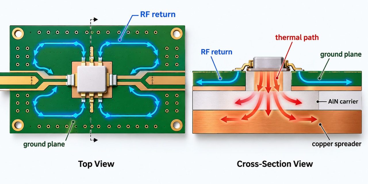
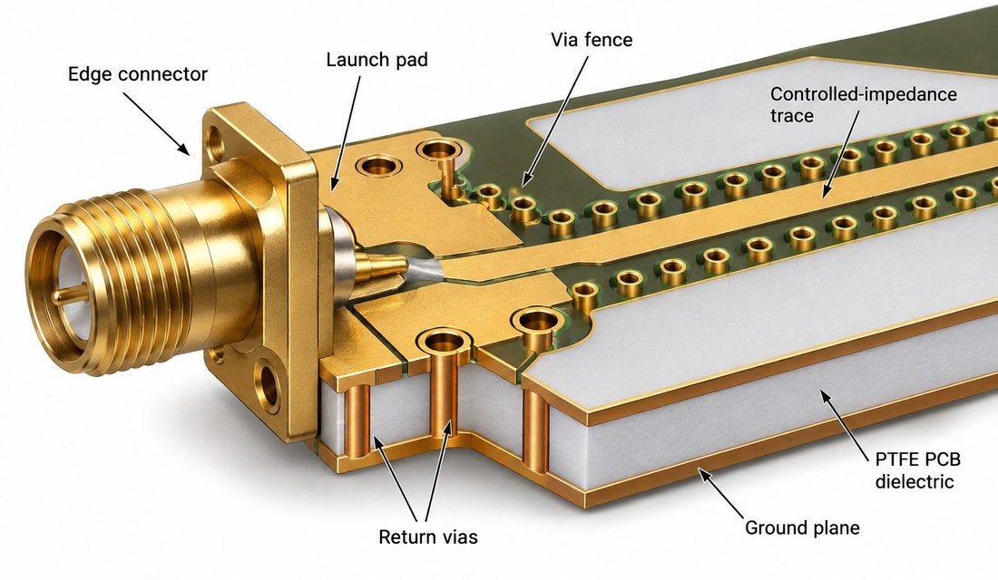
An Aluminum Nitride PCB sensor carrier must keep package geometry, RF return, and thermal margin visible in one controlled interface drawing. An mmWave sensor carrier must keep the feed geometry stable while moving heat away from the active device and preserving the enclosure datum. Aluminum nitride can support that combination, yet the first build can...

Aluminum Nitride PCB Direct-Bond Copper: Metallization and Via Reliability Before Qualification

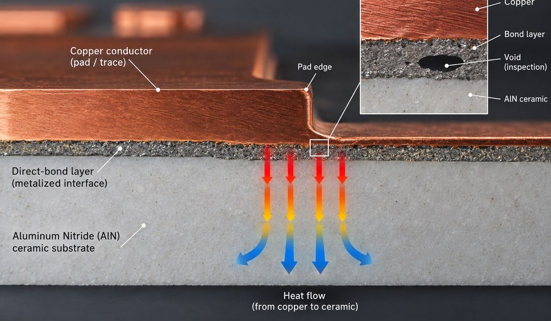
An Aluminum Nitride PCB direct-bond copper release needs a controlled metallization edge, via transition, and inspection record before qualification. Direct-bond copper can deliver a low-resistance thermal and electrical interface on aluminum nitride, but its edge, adhesion, and transition features must survive the same thermal history as the product. A qualification coupon that omits the heavy...

Aluminum Nitride PCB RF Power Layout: Separating Return Current from Heat Spreading

An Aluminum Nitride PCB power layout must release current return and heat through the same controlled interface before the module is approved. RF power boards built on aluminum nitride combine a low-loss electrical path with a high-conductivity thermal path, but the two paths do not always want the same copper geometry. A power island may...

Aluminum Nitride PCB Thermal Paths for RF Power: Releasing Copper and Carrier Interfaces

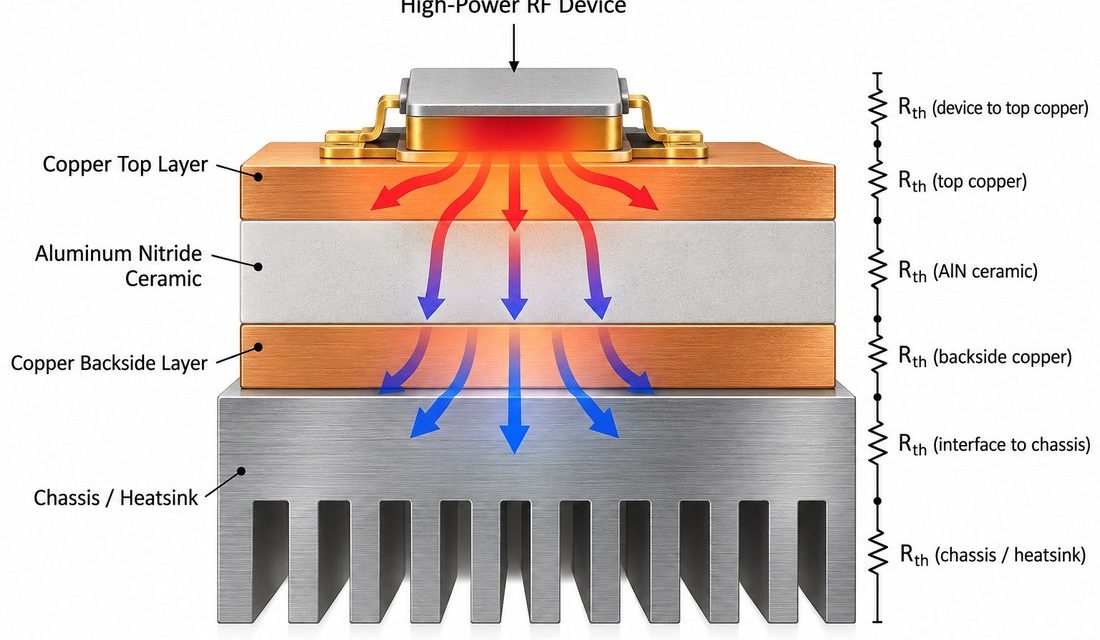
A power amplifier module can have a favorable ceramic thermal value and still miss its temperature margin because the heat path is not released as a complete assembly. An Aluminum Nitride PCB shares heat and RF functions with copper, solder or braze, a carrier, and the enclosure. The project pain is usually an interface assumption:...

Alumina PCB High-Power Reliability: Thermal Cycling, Copper Stress, and Interface Design

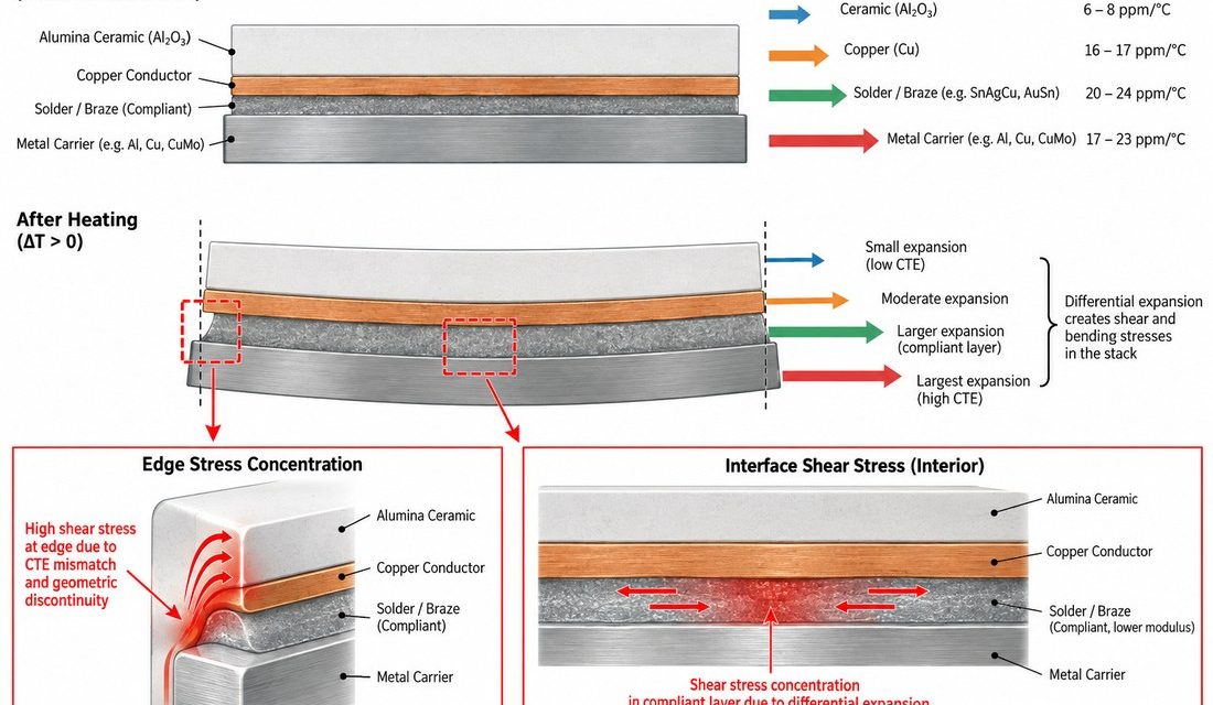
A high-power Alumina PCB can carry heat efficiently only when the copper, substrate, solder or braze, and metal carrier move together. Repeated temperature change makes the interface a mechanical system. The most common project mistake is to qualify the ceramic coupon while the product uses a different copper area, fastener pattern, or thermal interface. A...

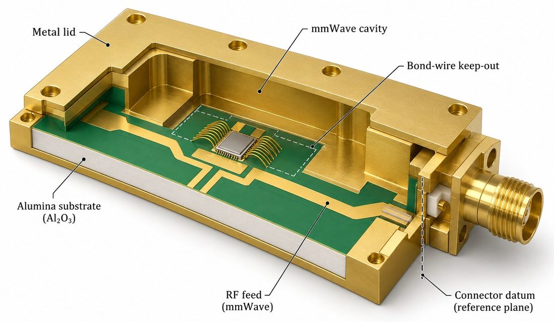
Alumina PCB for mmWave Packaging: Cavity, Ground, and Connector Datum Control

In a compact mmWave package, the Alumina PCB is often both circuit carrier and mechanical reference. A cavity, lid, bond window, connector, or waveguide transition can define the electromagnetic boundary more strongly than a long trace. The project risk is a datum mismatch: the electrical drawing references the board edge while the housing references the...

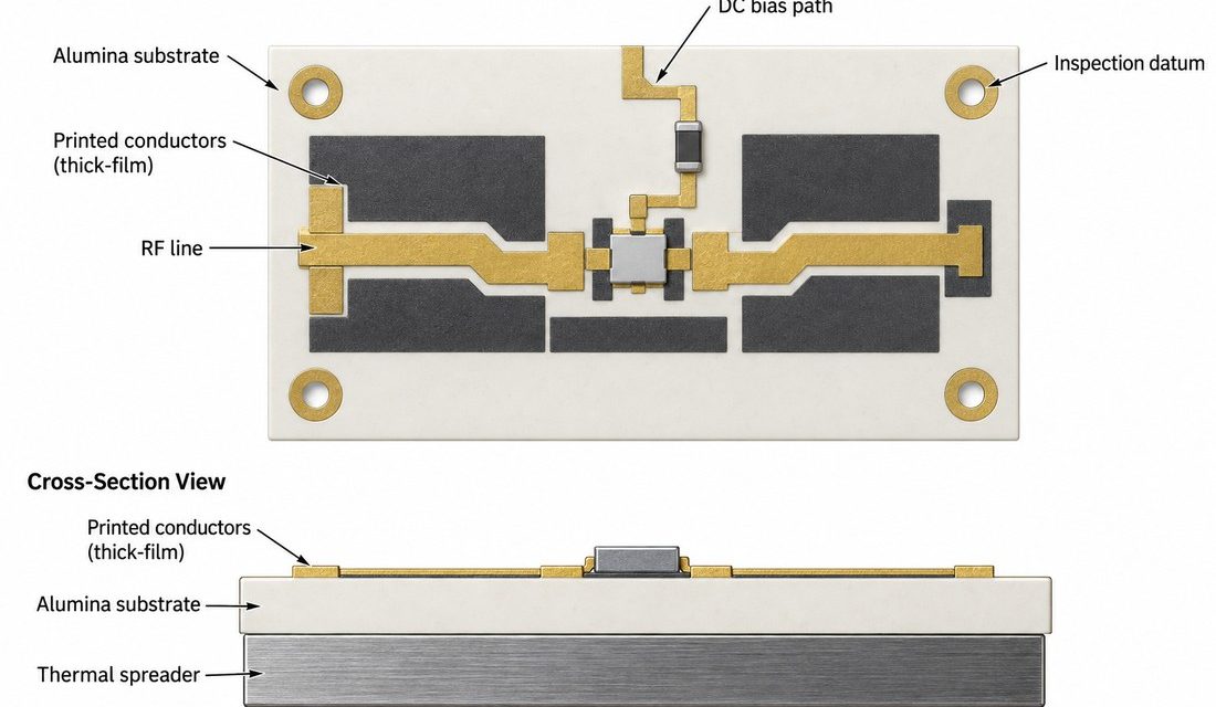
Alumina PCB Thick-Film RF Modules: Balancing Thermal Spreading and Layout Density

Alumina remains a practical ceramic substrate for RF modules, sensor hybrids, and compact power interfaces because it combines electrical insulation with a stable mechanical base. The challenge is density. A Alumina PCB can carry thick-film conductors, thin-film features, soldered parts, and a thermal interface in a small area, but every added pad or crossover changes...