
A power amplifier module can have a favorable ceramic thermal value and still miss its temperature margin because the heat path is not released as a complete assembly. An Aluminum Nitride PCB shares heat and RF functions with copper, solder or braze, a carrier, and the enclosure. The project pain is usually an interface assumption: the design team budgets the substrate, while the production unit adds voids, fastener load, surface flatness, and a return path that was never reviewed with the thermal drawing.
Map the thermal boundary before selecting copper
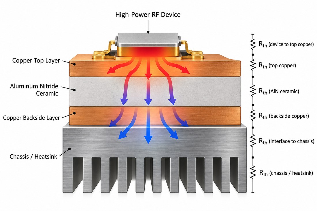
Start at the device attach or exposed pad and map every layer to the chassis: top metallization, AlN ceramic, backside copper, interface material, carrier, and fastener. The Aluminum Nitride PCB selection is only one term in the thermal resistance chain. Mark supplier typical values separately from the design target and from any acceptance value that will be measured on the finished module.
Copper spread improves heat flow but changes stiffness and current distribution. Keep the RF launch, ground return, and high-current thermal region in one coordinate system so a pad or slug change cannot silently move the reference plane. The thermal management review should show pad geometry, via or metallized transition, interface flatness, and the inspection location for voids or non-wet areas.
If the module uses a carrier or lid, define the mating datum, clamp or screw pattern, and compliant layer in the mechanical package. A thermal simulation can guide the target, but it cannot replace a released interface drawing.
Coordinate RF return with the heat spreader
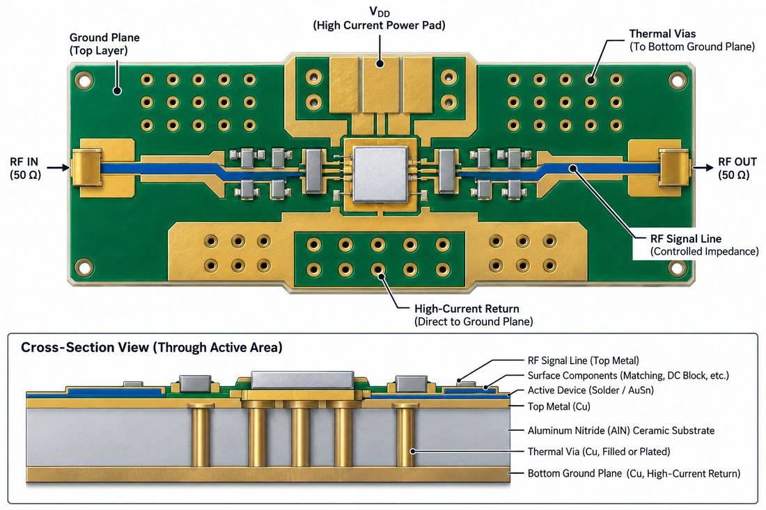
A broad copper area is not automatically a quiet RF reference. Slots, mounting holes, or an isolated power island can interrupt return current beneath a launch. The Aluminum Nitride PCB layout should identify signal vias, ground vias, thermal vias, and any shared barrel or metallized feature.
Keep the feed transition short and surround it with a deliberate return pattern. Analog Devices guidance treats a low-inductance return as a layout requirement; adapt that principle to the actual AlN metallization and via process quoted by the fabricator. The RF PCB drawing should call out the controlled region rather than relying on a generic ground-pour note.
When a thermal spreader crosses a carrier seam, review the three-dimensional current path and the mechanical constraint together. Release the design target, coupon geometry, and measurement fixture assumptions before the first build.
Make assembly evidence part of the release
Define the attach method, paste or braze condition, reflow or firing window, support points, and cleaning limits. A ceramic surface can be electrically stable while an uneven interface creates a local hot spot or a stress concentration. The controlled impedance handoff should state which evidence is required for the product feature and which is only a witness coupon.
For a first build, use a cross-section plan that covers the device pad, ceramic interface, backside copper, and carrier. Record sample identity and fixture conditions before calling a result measured. Keep the Aluminum Nitride PCB material revision, copper construction, and interface material synchronized in the bill of materials.
Close with a checklist: thermal path mapped, RF return continuous, interface datum defined, assembly process window agreed, and change owner named. This gives engineering and procurement a defensible decision gate.
An Aluminum Nitride PCB is reliable when ceramic, copper, carrier, and RF return are released as one physical boundary. Freeze the interfaces early, then use coupons and cross-sections to verify the process that the product actually uses.
Engineering release note: keep the thermal interface, RF reference, and inspection datum visible in the same revision-controlled package. When a device, copper feature, carrier, or assembly step changes, identify the affected assumption and repeat only the evidence tied to that boundary. This prevents a typical material value from being mistaken for a guaranteed product result.
Release note: keep the Aluminum Nitride PCB heat path, copper interface, and carrier datum together in the release package so thermal assumptions survive fabrication.
Sources: CeramTec aluminum nitride substrate data; Analog Devices RF and mixed-signal PCB layout guidance; supplier application notes for direct-bond copper and high-power ceramic modules. Numerical values are treated as typical supplier values, design targets, or engineering ranges unless a released drawing defines a measured acceptance value.
Release gate: document the Aluminum Nitride PCB interface before approval.
Release gate: document the Aluminum Nitride PCB interface before approval.
Release gate: return the PCB manufacturing evidence with the lot package.
Release gate: return the PCB assembly evidence with the lot package.
