
Alumina remains a practical ceramic substrate for RF modules, sensor hybrids, and compact power interfaces because it combines electrical insulation with a stable mechanical base. The challenge is density. A Alumina PCB can carry thick-film conductors, thin-film features, soldered parts, and a thermal interface in a small area, but every added pad or crossover changes the heat path and the return current. The project needs a layout method that exposes those interactions before the substrate is ordered.
Choose the conductor system with the module function
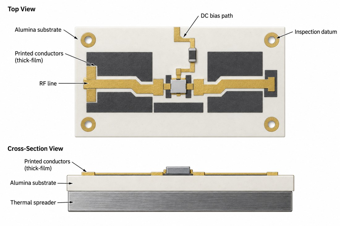
Separate high-frequency lines, DC distribution, heater or sensor elements, and mechanical pads in the floorplan. The Alumina PCB conductor process should be selected with the required line width, spacing, adhesion, and surface finish in mind. A conductor that is adequate for a low-current sensor trace may be unsuitable for a high-power RF path or a wire-bond landing.
Create a thermal map that starts at the active device and ends at the carrier. The RF PCB material review should state the alumina grade and supplier typical thermal value, then identify the interface resistance and mounting constraint as separate terms. Do not infer a junction temperature from substrate data alone.
Keep the RF return near the signal and avoid routing a heater, bias line, or fast digital edge through the same reference region without an isolation plan.
Use layout density without hiding inspection access
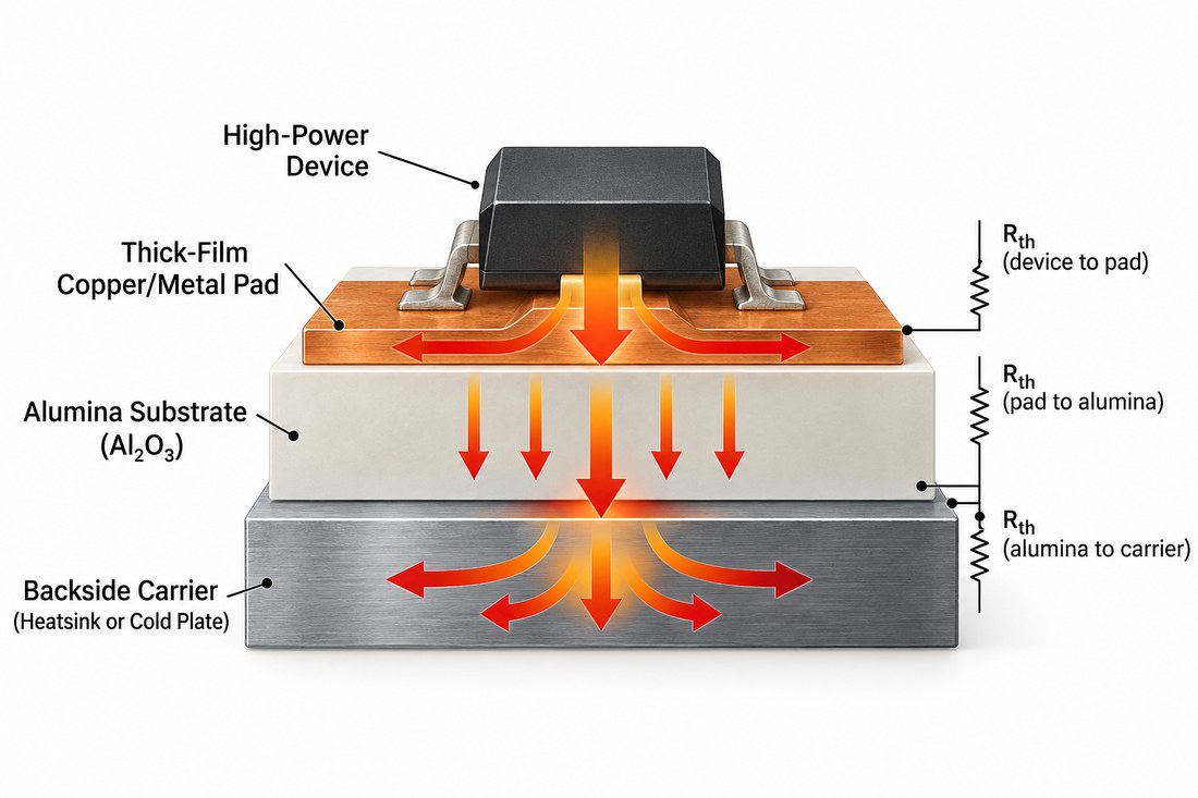
Compact hybrids often place parts close to a cavity or shield wall. Leave inspection access for conductor continuity, wire bond, solder fillet, and the thermal interface. A Alumina PCB drawing that is dense but not inspectable will create rework risk even if the artwork is correct.
The controlled impedance design page should identify the datum for wire-bond pads and the keep-out around the bond loop. For soldered components, define pad finish, paste access, and the expected fillet direction.
If a crossover or jumper is unavoidable, document its electrical and assembly purpose. Do not rely on a generic thick-film rule when the feature sits inside an RF launch or high-temperature zone.
Validate thermal and RF behavior as separate gates
Use one evidence plan for geometry and conductor inspection and another for RF or thermal performance. A cross-section or visual record can confirm a printed feature, but it cannot prove insertion loss or device temperature without a defined fixture and test method.
The thermal management manufacturing handoff should include screen or mask revision, firing or cure conditions when applicable, substrate thickness, and the location of any witness coupon. If the process changes, repeat the affected gate instead of carrying old evidence forward.
Close the design with a density map, return-path review, thermal-interface note, and inspection route. That gives the project manager a clear reason to approve the next build.
An Alumina PCB is most reliable when layout density is treated as a system constraint. Coordinate conductor technology, heat spreading, RF return, and inspection access before committing the thick-film artwork.
Implementation note for this thick-film RF and thermal spreading review: keep the engineering assumption visible at the point where it affects a drawing, a supplier quote, or an inspection record. Ask the design owner to identify the reference plane, interface datum, and acceptance method before the release is frozen. Ask manufacturing to return the proposed stack, panel, and process window rather than a generic capability statement. Ask assembly to identify the profile, cleaning, and support conditions that could move the RF or thermal result. This simple handoff prevents a typical material value from being mistaken for a guaranteed product result and gives the project team a clear action when an ECO changes the physical boundary.
Release note: keep the Alumina PCB conductor pattern, thermal interface, and thick-film process in one released drawing so density decisions remain traceable to heat-spreading needs.
Sources: Panasonic MEGTRON technical material guidance; Rogers and Taconic high-frequency material data sheets where relevant; CeramTec ceramic substrate data; Analog Devices RF and mixed-signal layout guidance. Numerical values are treated as typical supplier values or engineering targets unless the released drawing defines a measured acceptance value.
Release note: confirm the Alumina PCB construction before the next ECO.
Release note: confirm the Alumina PCB construction before the next ECO.
Release note: confirm the PCB manufacturing evidence before approval.
Release note: confirm the PCB assembly evidence before approval.
