
In a compact mmWave package, the Alumina PCB is often both circuit carrier and mechanical reference. A cavity, lid, bond window, connector, or waveguide transition can define the electromagnetic boundary more strongly than a long trace. The project risk is a datum mismatch: the electrical drawing references the board edge while the housing references the machined pocket, or the ground wall is interrupted by an assembly keep-out.
Choose one datum system for the RF package
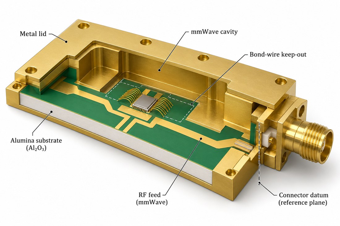
Create a package drawing that identifies the antenna or waveguide aperture, cavity wall, connector axis, and mounting features. The Alumina PCB substrate should have a controlled edge or metallized wall where the RF boundary depends on it. Do not let the board supplier and the housing supplier create independent coordinate systems.
The RF PCB design review should show the cavity depth, lid spacing, bond-wire keep-out, and any coating or adhesive allowed near the field. Use supplier capability information to choose the tolerances; mark each dimension as electrical, mechanical, or inspection-critical.
When a connector is soldered or brazed, make its coplanarity and pin position part of the package datum. A few tenths of a millimeter at a launch can matter more than a long low-loss line elsewhere.
Keep the return wall continuous
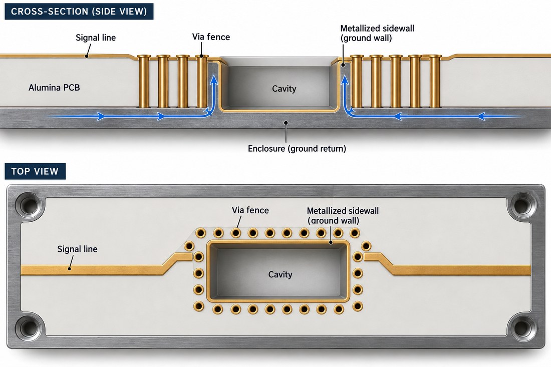
Ground vias, sidewall metallization, and the lid contact form the return boundary. The Alumina PCB layout should show where current crosses between the substrate, carrier, and enclosure. Analog Devices grounding guidance is a useful reminder that return current follows impedance, not a schematic label.
Place ground features close to signal transitions and protect them from solder mask, adhesive, and mechanical cutouts. The controlled impedance fabrication note should identify the sidewall or via process and the inspection evidence required for continuity.
If the package includes multiple RF channels, define a partition strategy and the allowed coupling path. A ground wall that is continuous electrically but interrupted mechanically may still leak at the operating frequency.
Verify the package before tuning the circuit
Build a correlation plan that records the fabricated cavity, connector, and lid dimensions before interpreting the RF response. Keep a clear distinction between a design target, a supplier typical value, and a measured sample result.
The thermal management assembly handoff should state the sequence for bonding, soldering, cleaning, and lid attachment. Sequence changes can move the connector or change the cavity gap.
Freeze the package revision with the stackup, aperture, ground-wall, and connector checklist. This avoids tuning a prototype to a geometry that procurement cannot repeat.
An Alumina PCB mmWave package is a combined RF and mechanical component. One datum system, a continuous return boundary, and measured geometry evidence are the safest way to protect the first build.
Implementation note for this mmWave packaging and cavity review: keep the engineering assumption visible at the point where it affects a drawing, a supplier quote, or an inspection record. Ask the design owner to identify the reference plane, interface datum, and acceptance method before the release is frozen. Ask manufacturing to return the proposed stack, panel, and process window rather than a generic capability statement. Ask assembly to identify the profile, cleaning, and support conditions that could move the RF or thermal result. This simple handoff prevents a typical material value from being mistaken for a guaranteed product result and gives the project team a clear action when an ECO changes the physical boundary.
Release note: keep the Alumina PCB cavity datum, ground wall, and connector reference in the same package drawing so mmWave alignment survives supplier handoff.
Sources: Panasonic MEGTRON technical material guidance; Rogers and Taconic high-frequency material data sheets where relevant; CeramTec ceramic substrate data; Analog Devices RF and mixed-signal layout guidance. Numerical values are treated as typical supplier values or engineering targets unless the released drawing defines a measured acceptance value.
Release note: confirm the Alumina PCB construction before the next ECO.
Release note: confirm the Alumina PCB construction before the next ECO.
Release note: confirm the Alumina PCB construction before the next ECO.
Release note: confirm the PCB manufacturing evidence before approval.
Release note: confirm the PCB assembly evidence before approval.
