HomeCategory

Advanced Engineering Technologies for PCB & PCBA Solutions - KKPCB

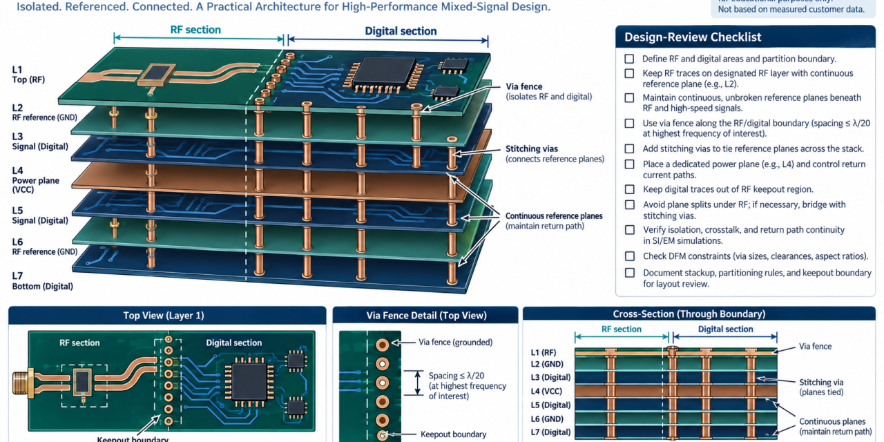
RF-35 PCB Mixed-Signal Stackup: Partitioning RF and Digital Return Paths

Mixed RF-and-digital boards rarely fail because the engineer forgot a trace-width rule. They fail when the stackup, plane strategy, and return path are treated as separate documents. This article uses an RF-35 PCB example to explain how a project team can partition RF and digital functions while keeping the board manufacturable. RF-35 ceramic-filled PTFE/glass materials...
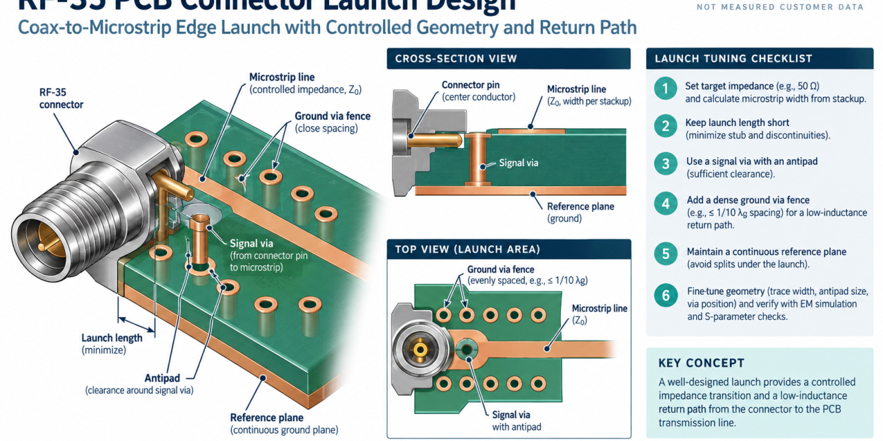
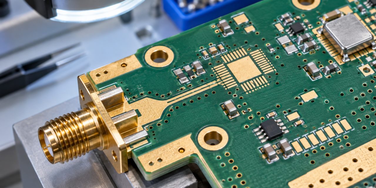
RF-35 PCB Connector Launch and Via Transition: A Practical Verification Workflow

A connector launch is the shortest and most fragile transmission-line section on many microwave boards. The signal leaves a coaxial pin, crosses a pad and via, and then enters a controlled planar line. This guide uses an RF-35 PCB example to show how to release that transition with a defined return path, manufacturable clearances, and...

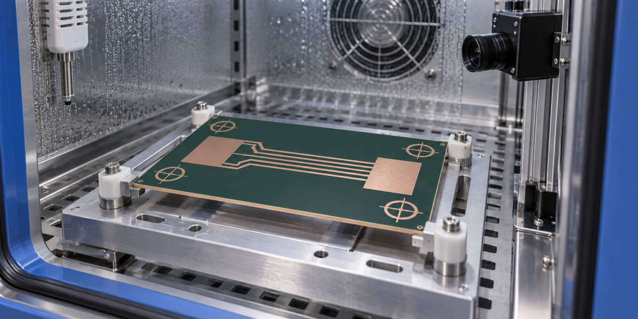
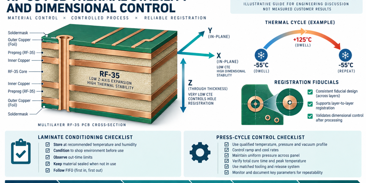
RF-35 PCB Thermal Stability: Controlling CTE, Registration, and Drill Reliability

Thermal drift is an electrical problem when a microwave board moves enough to change trace geometry, connector alignment, or plated-hole stress. This article treats RF-35 PCB as a production material choice and focuses on the thermal-mechanical controls that keep a high-frequency design repeatable from panel build through assembly. Taconic RF-35 typical property tables report a...

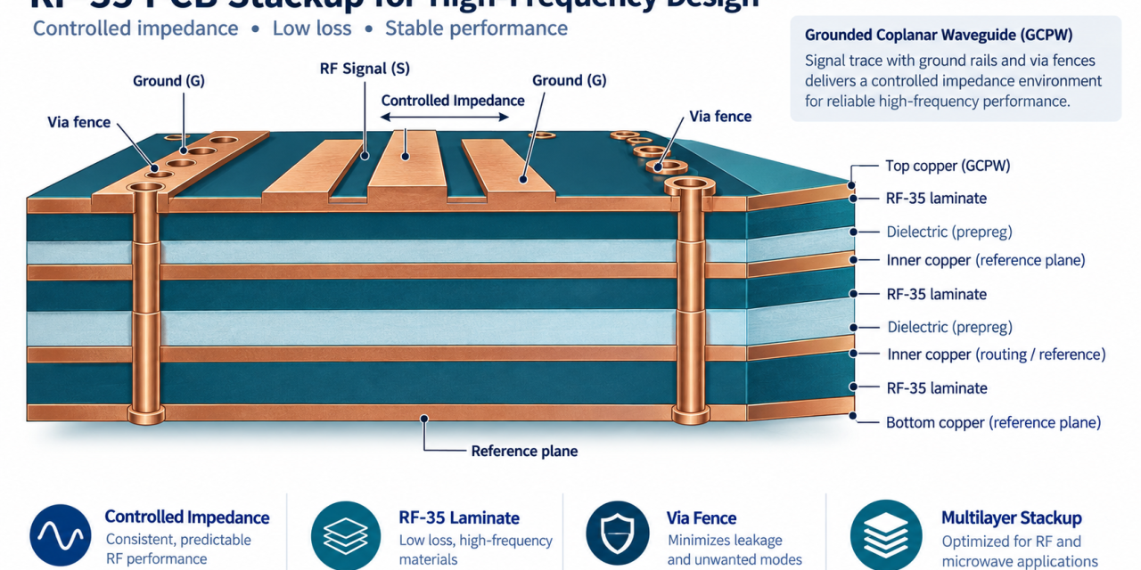
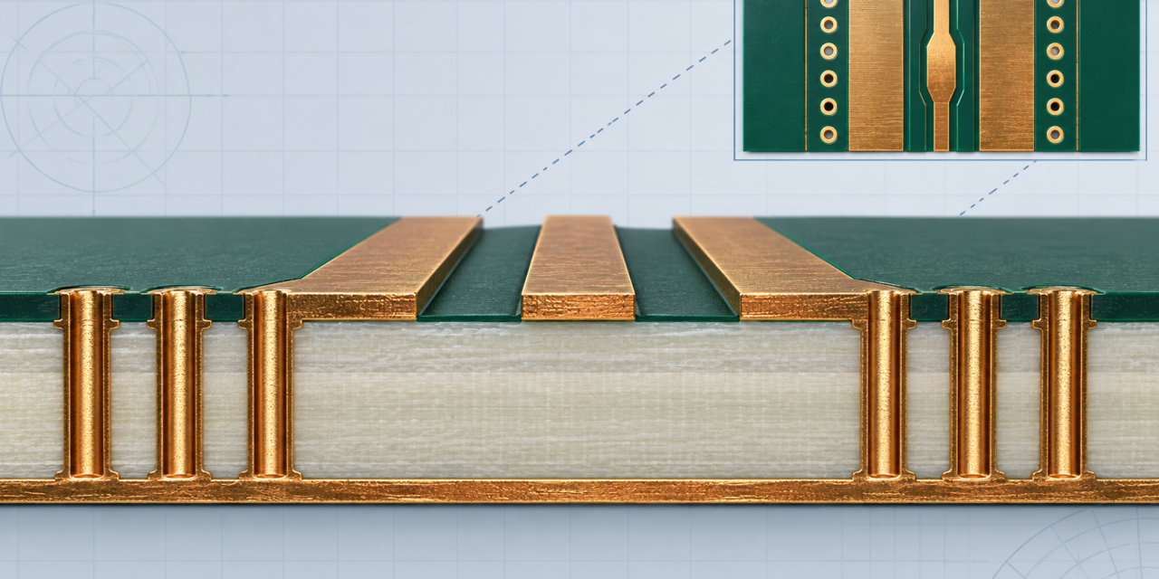
RF-35 PCB Stackup and Controlled-Impedance Release for High-Frequency Designs

High-frequency board projects often fail at the handoff between an electrical stackup and a buildable panel. A designer may select a low-loss laminate, but the fabricator still needs a controlled dielectric thickness, a stable reference plane, and a practical drill-and-plate sequence. This guide uses an RF-35 PCB design example to show how to convert an...

RO5880 PCB Dimensional Stability: Managing Moisture and Registration in Outdoor Radar

Outdoor radar and microwave equipment can see humidity, temperature swings, and repeated handling before a board reaches final system test. For a PTFE-based laminate, the project risk is not only RF loss; it is whether the finished RO5880 PCB keeps its layer registration, connector datum, and antenna geometry through the approved process. This RO5880 PCB...