
An Aluminum Nitride PCB power layout must release current return and heat through the same controlled interface before the module is approved.
RF power boards built on aluminum nitride combine a low-loss electrical path with a high-conductivity thermal path, but the two paths do not always want the same copper geometry. A power island may need wide metal while a microwave launch needs a clean reference plane. When the project team treats both as one undifferentiated pour, the first prototype can show unexpected coupling, connector mismatch, or thermal stress at the ceramic edge. This review gives a layout and release method for separating those risks without losing the benefit of the substrate.
Partition the RF and power regions
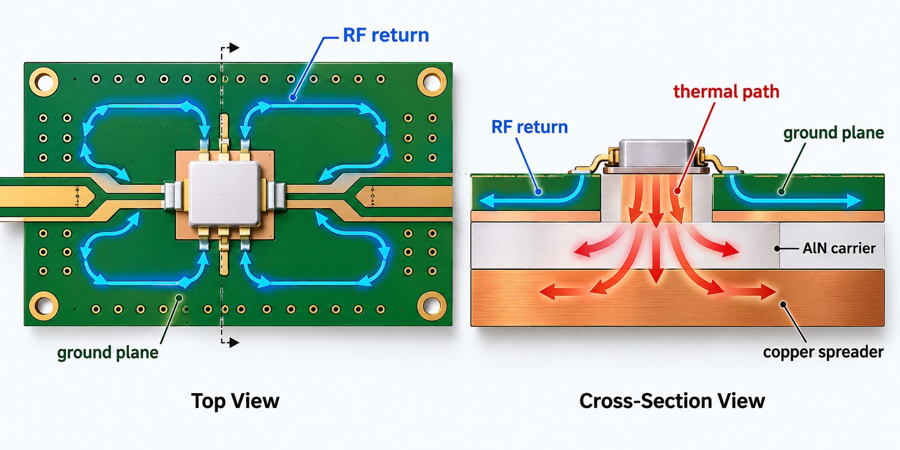
Define the RF launch, active device land, bias network, high-current feed, and thermal spreader in the floorplan. The Aluminum Nitride PCB board should have a named reference plane for every controlled line and a clear boundary where power copper expands. Keep the current-return path short and visible rather than assuming that a large backside plane solves every transition.
Use the device package and connector datum as the first coordinates, then add ground vias or metallized features near the feed. The thermal management review should identify where a power via may share a thermal region and where it must remain outside the RF launch. Mark any slot or mounting hole that can change the return path.
A field-solver result can be a design target, but the production drawing still needs pad, drill, clearance, and inspection dimensions that the ceramic process can hold.
Control copper-to-ceramic strain
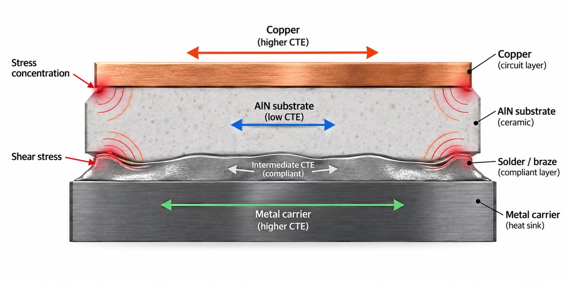
Large copper areas create a useful heat spreader and a mechanical constraint. Compare the CTE assumptions for copper, AlN, solder or braze, and the carrier. The Aluminum Nitride PCB assembly should show compliant interfaces, neutral-axis assumptions, and support locations before the thermal design is frozen.
Avoid a narrow copper neck between a high-current pad and the spreader. That neck can create both a thermal bottleneck and a stress concentration. The RF PCB manufacturing note should state copper thickness, bond or attach method, flatness, and which edge features are inspection-critical.
When a power change alters copper density, repeat the RF return review and the mechanical tolerance stack. A power ECO is not electrically local when it changes the reference conductor or carrier load.
Release a combined electrical and mechanical checklist
Require the package to include a stack or cross-section, RF launch detail, power map, thermal interface drawing, and inspection plan. The controlled impedance handoff should distinguish typical material properties, design targets, and measured acceptance evidence.
Use a representative coupon only when it follows the same metallization and assembly history as the product. Keep the Aluminum Nitride PCB identifier and supplier data-sheet revision in the drawing title block and purchase order.
Before volume release, review the return path, thermal path, carrier constraint, connector datum, and change triggers together. This short gate is more useful than adding a generic “high-power capable” note.
Aluminum Nitride PCB RF power layout is a current-return and interface problem as much as a routing problem. Partition the regions, control copper strain, and release evidence that matches the finished module.
Engineering release note: keep the thermal interface, RF reference, and inspection datum visible in the same revision-controlled package. When a device, copper feature, carrier, or assembly step changes, identify the affected assumption and repeat only the evidence tied to that boundary. This prevents a typical material value from being mistaken for a guaranteed product result.
Release note: keep the Aluminum Nitride PCB RF return path separate from the heat-spreading interface in the drawing and inspection plan.
Sources: CeramTec aluminum nitride substrate data; Analog Devices RF and mixed-signal PCB layout guidance; supplier application notes for direct-bond copper and high-power ceramic modules. Numerical values are treated as typical supplier values, design targets, or engineering ranges unless a released drawing defines a measured acceptance value.
Release gate: document the Aluminum Nitride PCB interface before approval.
Release gate: document the Aluminum Nitride PCB interface before approval.
Release gate: return the PCB manufacturing evidence with the lot package.
Release gate: return the PCB assembly evidence with the lot package.
