
An Aluminum Nitride PCB direct-bond copper release needs a controlled metallization edge, via transition, and inspection record before qualification.
Direct-bond copper can deliver a low-resistance thermal and electrical interface on aluminum nitride, but its edge, adhesion, and transition features must survive the same thermal history as the product. A qualification coupon that omits the heavy copper edge, via array, or carrier bond does not answer the production question. The engineering task is to separate the electrical role of each metal feature from the mechanical strain that qualification will expose.
Identify every metallization role
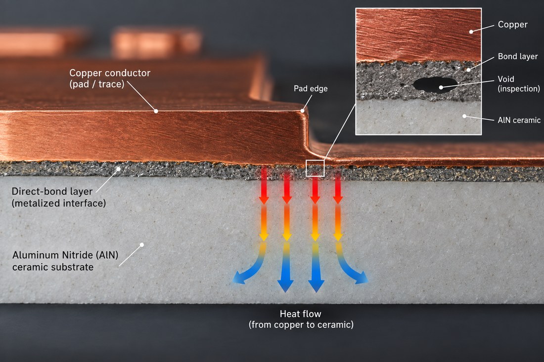
Create a feature map for signal traces, thermal pads, ground transitions, power bus copper, mounting holes, and any bond or plated via. The Aluminum Nitride PCB drawing should state the copper construction, bond interface, finished thickness target, and allowed edge condition. Do not use a single generic via note for signal, thermal, and mechanical features.
For direct-bond copper, show the ceramic boundary, copper edge, transition radius, and inspection access in a cross-section. The thermal management specification should identify which values are supplier typical and which dimensions are acceptance limits. If the design depends on a flat interface, call out the datum and measurement method.
Keep high-frequency transitions away from a copper edge or carrier seam unless the return path has been reviewed in three dimensions. A mechanically sound bond can still be a poor RF transition.
Design the via and edge for thermal cycling
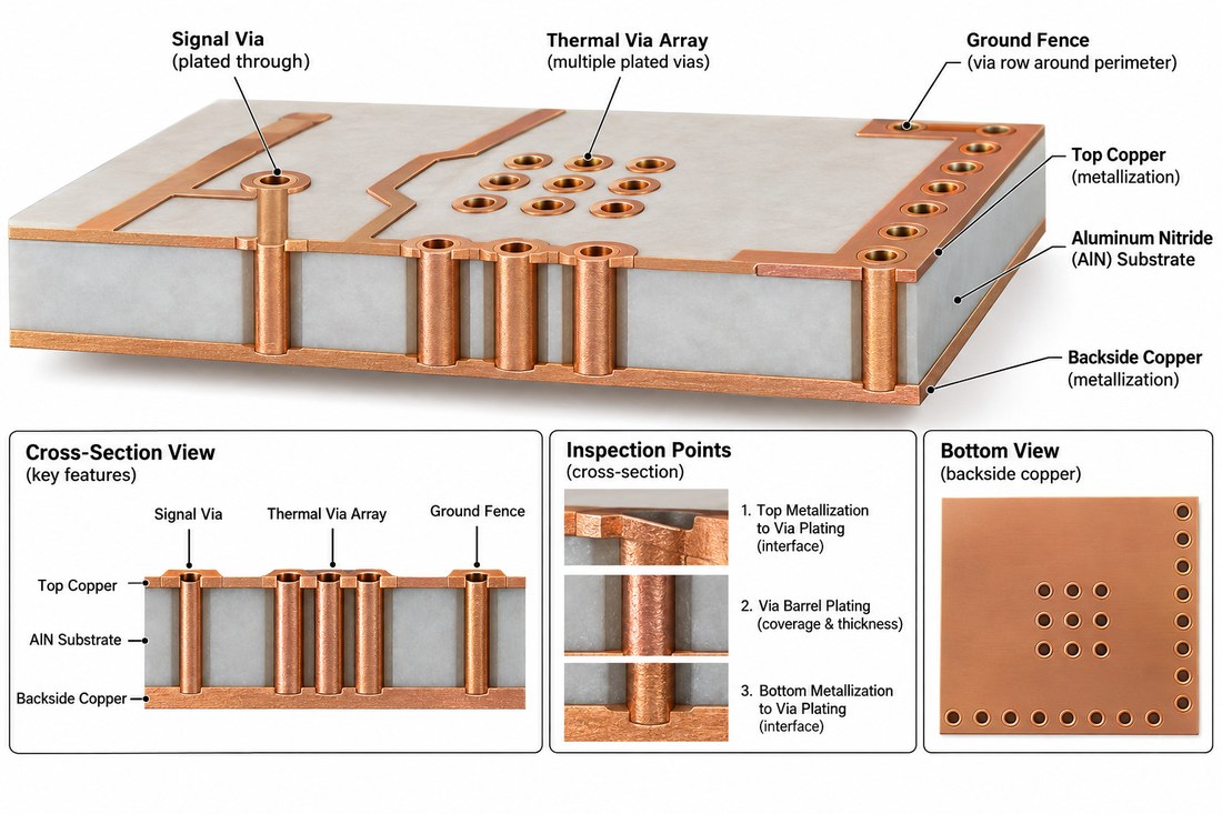
AlN, copper, solder or braze, and a metal carrier expand differently. Concentrated stress can appear at a via corner, copper step, or edge metallization. The Aluminum Nitride PCB layout should show keep-outs, compliant regions, and the expected neutral axis when a board is mounted.
Use a representative thermal-cycle plan with product-like copper area, carrier constraint, and attach sequence. The RF PCB quality plan should specify cross-section locations, continuity checks, void inspection, and how a crack or delamination is classified. A coupon result is evidence of the sampled process, not a universal guarantee.
Spread current before it enters a small neck and keep return vias near the RF launch. Do not force ground and power vias into one stress concentration without a mechanical review.
Control substitutions and qualification evidence
A proposed change to copper thickness, bond layer, paste, plating, or via fill must trigger an impact review. The controlled impedance procurement note should require engineering approval when a substitute changes thermal resistance, CTE, dielectric boundary, or metallization adhesion.
Keep lot traceability tied to the material revision, copper process, and inspection record. The Aluminum Nitride PCB identifier belongs in the bill of materials and drawing title block so a buyer cannot silently replace it with a visually similar ceramic.
Close the gate with a feature map, cross-section plan, thermal-cycle profile, acceptance limits, and deviation owner. This turns direct-bond copper from a material claim into a controlled production interface.
Aluminum Nitride PCB qualification is credible only when the coupon represents the product’s copper edge, via array, carrier, and attach process. Define those features before approving the first lot.
Engineering release note: keep the thermal interface, RF reference, and inspection datum visible in the same revision-controlled package. When a device, copper feature, carrier, or assembly step changes, identify the affected assumption and repeat only the evidence tied to that boundary. This prevents a typical material value from being mistaken for a guaranteed product result.
Release note: keep the Aluminum Nitride PCB direct-bond copper stack, metallization method, and via evidence tied to the same qualification revision.
Sources: CeramTec aluminum nitride substrate data; Analog Devices RF and mixed-signal PCB layout guidance; supplier application notes for direct-bond copper and high-power ceramic modules. Numerical values are treated as typical supplier values, design targets, or engineering ranges unless a released drawing defines a measured acceptance value.
Release gate: document the Aluminum Nitride PCB interface before approval.
Release gate: document the Aluminum Nitride PCB interface before approval.
Release gate: return the PCB manufacturing evidence with the lot package.
Release gate: return the PCB assembly evidence with the lot package.
