HomeCategory

PCB Design Services | Professional PCB Layout & Design - KKPCB

Introduction to PCB Design

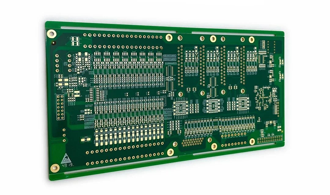
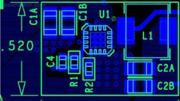
PCB design involves two critical stages: component layout and circuit connection wiring. The layout is the arrangement of circuit components within the PCB’s wiring area. A well-thought-out layout directly affects the ease of subsequent wiring and significantly impacts the PCB’s overall performance. In addition to meeting circuit functionality and performance requirements, a good layout considers manufacturability, inspection, and maintenance....

Electromagnetic Compatibility Design of Mobile Phone PCB

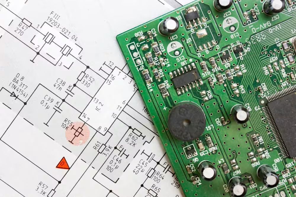
With the continuous development of smartphones toward higher performance, smaller size, and increased functionality, mobile phone PCB design has become more complex than ever. Modern smartphones integrate high-speed processors, RF communication modules, cameras, sensors, power management circuits, and high-density interconnect structures within extremely limited space. However, increasing circuit density and operating frequencies also introduce greater...

The Five Golden Rules of PCB Design

Printed Circuit Board (PCB) design is a critical step in the development of any electronic product. A well-designed PCB ensures reliability, performance, and manufacturability, while a poor design can lead to costly failures and delays. Below are five golden rules that every PCB designer should follow. 1. Prioritize Clear and Logical Layout A clean and...

10 Key Steps to Ensure Signal Integrity (SI) in PCB Design

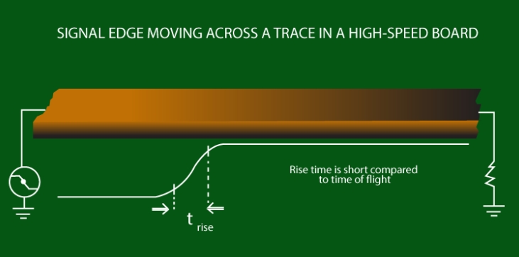
Introduction: Addressing signal integrity (SI) issues early in the PCB design process can streamline the design and eliminate the need for corrective termination devices later. Here, we outline critical steps to maintain signal integrity, from planning through testing. 1. Preparation Before Design Begin by defining your SI requirements and design strategy. Early-stage planning will guide component selection,...

Relationship Between Current and Line Width in PCB Design

In PCB design, trace width is one of the fundamental parameters that directly affects the electrical performance, thermal reliability, and manufacturing quality of a circuit board. When current flows through a PCB trace, the conductor generates heat due to electrical resistance. If the trace width is insufficient, excessive temperature rise may cause: Copper trace overheating...

Multilayer PCB Manufacturing Process: A Complete Step-by-Step Guide

With the increasing demand for higher circuit density, faster signal transmission, and more complex electronic functions, multilayer printed circuit boards (PCBs) have become a fundamental technology in modern electronic products. Unlike single-layer or double-sided PCBs, multilayer PCBs integrate multiple copper layers and insulating dielectric materials into one compact structure, allowing engineers to achieve complex routing,...

PCB for SMT (Surface Mount Technology): Choosing the Right PCB for SMD Components

With the rapid development of electronic products toward miniaturization, higher integration, and automated manufacturing, Surface Mount Technology (SMT) has become one of the most widely used PCB assembly methods in modern electronics. Unlike traditional through-hole components, Surface Mount Devices (SMD components) are mounted directly onto the surface of a PCB, allowing manufacturers to achieve: Higher...

PCB Layout Planning – Packages and Routing

PCB layout planning is a critical phase in the design process, enabling engineers to save time and ensure a structured approach to package management, component placement, and routing. Proper planning ensures that the design meets electrical, spacing, and physical requirements before moving to the actual layout stage. This article explores key aspects of PCB layout planning, focusing on footprint management, routing strategies,...