
In PCB design, trace width is one of the fundamental parameters that directly affects the electrical performance, thermal reliability, and manufacturing quality of a circuit board.
When current flows through a PCB trace, the conductor generates heat due to electrical resistance. If the trace width is insufficient, excessive temperature rise may cause:
- Copper trace overheating
- Voltage drop
- Reduced electrical efficiency
- PCB reliability issues
- Potential circuit failure
Therefore, understanding the relationship between current capacity and PCB trace width is essential for designing reliable power circuits, high-current boards, and industrial electronic systems.
A proper trace width design requires consideration of multiple factors, including:
- Current level
- Copper thickness
- Allowable temperature rise
- Trace length
- PCB material
- Environmental conditions
1. Basic Relationship Between Current and PCB Trace Width
PCB traces are essentially copper conductors. Similar to wires, their ability to carry current depends largely on their cross-sectional area.
The cross-sectional area of a PCB trace is determined by:
- Trace width
- Copper thickness
A wider trace provides:
- Lower resistance
- Lower heat generation
- Higher current carrying capability
The relationship can be summarized as:
Higher Current → Larger Copper Area Required → Wider Trace or Thicker Copper Layer
For low-power signal circuits, narrow traces may be sufficient. However, power supply paths and high-current circuits require wider traces to maintain reliability.
2. Factors Affecting PCB Current Carrying Capacity

2.1 Copper Thickness
Copper thickness is one of the most important factors influencing current capacity.
Common PCB copper thickness values include:
- 1 oz copper (approximately 35μm)
- 2 oz copper (approximately 70μm)
- 3 oz copper (approximately 105μm)
A thicker copper layer provides:
- Lower resistance
- Better heat dissipation
- Higher current capacity
For high-current applications, designers may select heavier copper PCBs.
Examples:
- Battery management systems
- Motor controllers
- Power converters
2.2 Trace Width
Trace width determines the available conductive area.
A wider trace provides:
- Reduced resistance
- Lower voltage drop
- Improved thermal performance
For example:
A narrow trace carrying high current may experience:
- Excessive temperature rise
- Copper damage
- Reduced lifetime
A wider trace distributes heat more effectively.
2.3 Allowable Temperature Rise
Current flow causes heat generation.
PCB designers usually define an acceptable temperature rise, such as:
- 10°C
- 20°C
- 30°C
A higher allowable temperature rise allows more current through the same trace width.
However, excessive temperature increase may affect:
- Solder joints
- Component lifetime
- PCB reliability
2.4 Trace Length
Trace length also affects current performance.
Longer traces have:
- Higher resistance
- Greater voltage loss
- More heat generation
Short and wide power traces are preferred for high-current paths.
2.5 PCB Layer Position
The location of the trace influences heat dissipation.
External Layer Traces
Advantages:
- Better airflow cooling
- Easier heat dissipation
Internal Layer Traces
Challenges:
- Limited heat transfer
- Surrounded by dielectric material
Internal power traces may require additional copper area.
3. How to Calculate PCB Trace Width
PCB trace width calculation is usually based on:
- Current requirement
- Copper thickness
- Temperature rise allowance
The commonly used calculation methods are based on IPC standards, especially:
IPC-2221 PCB design guidelines
A simplified relationship considers:
- Current (I)
- Cross-sectional area (A)
- Temperature rise
The general principle:
Higher current requires a larger copper cross-sectional area.
Engineers often use PCB design software calculators to determine appropriate trace width based on specific requirements.
4. Typical PCB Trace Width Reference
The following values are general guidelines and should be verified according to actual design conditions.
| Current Level | Recommended Trace Consideration |
|---|---|
| Signal current (mA level) | Narrow traces are usually acceptable |
| 1A–2A | Medium-width traces depending on copper thickness |
| 3A–5A | Wider traces or thicker copper recommended |
| 10A+ | Heavy copper PCB, copper pours, or multiple layers required |
Actual requirements depend on:
- Copper thickness
- Ambient temperature
- Trace length
- Cooling conditions
5. Relationship Between Trace Width and Voltage Drop
Besides temperature rise, trace width affects voltage drop.
PCB traces have electrical resistance:
Where:
- R = resistance
- ρ = copper resistivity
- L = trace length
- A = conductor cross-sectional area
A narrower trace results in:
- Higher resistance
- Larger voltage drop
This is especially important in:
- Power supply circuits
- Battery systems
- Motor control boards
Stable voltage delivery requires carefully designed power traces.
6. PCB Trace Width Design for High-Current Applications
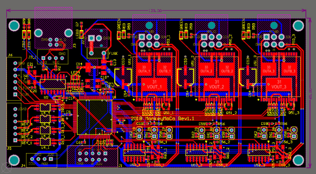
6.1 Use Wider Power Traces
For high-current paths:
- Increase trace width
- Increase copper thickness
- Use copper pours
Applications:
- DC power input
- Battery connections
- Motor drivers
6.2 Use Multiple Layers for Current Distribution
When a single layer cannot support required current, designers can:
- Connect multiple copper layers with vias
- Use parallel power paths
Benefits:
- Reduced resistance
- Improved thermal performance
6.3 Add Thermal Vias
Thermal vias help transfer heat between PCB layers.
They are useful for:
- Power MOSFETs
- Voltage regulators
- High-current components
6.4 Consider Copper Pour Design
Copper areas can improve:
- Current distribution
- Heat dissipation
- Ground performance
Common applications:
- Power planes
- Ground planes
- High-current return paths
7. Special Considerations for High-Frequency PCB Traces
Although wider traces improve current capacity, high-frequency PCB design requires additional considerations.
Increasing trace width may affect:
- Characteristic impedance
- Signal propagation
- Electromagnetic performance
For RF and microwave circuits, designers must balance:
- Current capacity
- Impedance control
- Signal integrity
8. Common PCB Trace Width Design Mistakes
8.1 Using Signal Trace Width for Power Paths
Problem:
A narrow signal trace is used for high-current applications.
Result:
- Excessive heating
- Voltage instability
- Reliability problems
8.2 Ignoring Temperature Rise
Problem:
Only current value is considered.
Result:
The PCB may operate beyond safe thermal limits.
8.3 Not Considering Copper Thickness
Problem:
Trace width is selected without considering copper weight.
Result:
Actual current capability may be insufficient.
8.4 Long Narrow Power Routing
Problem:
Long traces increase resistance.
Result:
- Greater voltage drop
- Higher power loss
9. Applications Requiring Careful Current and Trace Width Design
Power Electronics
Examples:
- DC/DC converters
- Inverters
- Motor controllers
Requirements:
- High current capacity
- Thermal reliability
Automotive Electronics
Examples:
- Battery management systems
- Electric vehicle controllers
Requirements:
- Long-term stability
- Environmental reliability
Industrial Control Systems
Examples:
- PLC boards
- Automation equipment
Requirements:
- Continuous operation
- High reliability
LED Lighting Systems
Requirements:
- Stable current distribution
- Heat management
10. Manufacturing Considerations
A trace width design must also match PCB manufacturing capabilities.
Important factors include:
Minimum Trace Width and Spacing
Manufacturing limitations affect:
- Production yield
- Cost
- Reliability
Heavy Copper PCB Capability
High-current applications may require:
- 2 oz copper
- 3 oz copper
- 4 oz or higher copper
Heavy copper PCBs improve current capacity but require specialized manufacturing processes.
DFM Review
Before production, engineers should verify:
- Current paths
- Thermal design
- Copper balance
- Manufacturing feasibility
Conclusion
The relationship between current and PCB trace width is a critical consideration in circuit board design.
A properly designed trace should balance:
- Current carrying capability
- Temperature rise
- Voltage drop
- Manufacturing requirements
- Product reliability
For low-power circuits, standard trace widths may be sufficient. However, power electronics, automotive systems, and industrial applications often require wider traces, thicker copper, and optimized thermal structures.
By understanding the relationship between current and line width, engineers can design PCBs with improved electrical performance, higher reliability, and longer service life.
