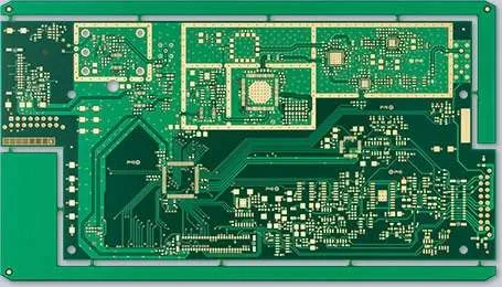
Multilayer PCBs (Printed Circuit Boards) are the heart of complex modern electronics, consisting of three or more conductive copper layers separated by insulating dielectric materials. Unlike simpler boards, they offer higher circuit density and improved signal integrity, making them essential for everything from smartphones to aerospace technology.
Step 1: Design and Data Preparation
The process begins with creating a board layout using CAD software. This design is exported into Gerber files, which define every detail, from copper traces to solder mask clearances. Engineers perform a Design for Manufacturing (DFM) check to ensure the files match the factory’s capabilities.
Step 2: Inner Layer Imaging and Etching
For the inner layers, a copper-clad core is cleaned and coated with a photosensitive film called photoresist. The circuit pattern is transferred to this film using UV light. After development, chemicals etch away the unwanted copper, leaving only the intended circuit traces.
Step 3: Automated Optical Inspection (AOI)
Before the layers are bonded, they undergo AOI. High-resolution cameras compare the physical inner layers against the original Gerber data to detect defects like shorts or open circuits.
Step 4: Lamination (Lay-up)
The inspected inner layers, insulating prepreg (fiberglass soaked in resin), and outer copper foils are stacked according to the design. This stack is placed in a vacuum press under extreme heat and pressure, which melts the resin and bonds all components into a single, solid structure.
Step 5: Drilling and Plating
Computer-controlled machines drill precise holes (vias) through the entire stack to create electrical connections between different layers. These holes are then chemically treated to deposit a thin layer of copper on their inner walls, a process known as electroless copper deposition.
Step 6: Outer Layer Processing
The outer layers undergo imaging and etching similar to the inner layers. Additional copper plating is often applied to thicken the conductive paths and the hole walls for better reliability.
Step 7: Solder Mask and Silkscreen
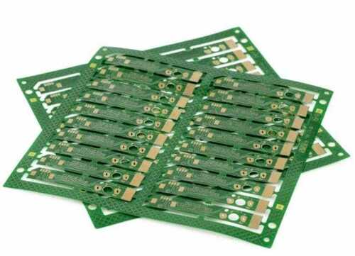
A protective solder mask (typically green) is applied to the entire board, leaving only the component pads exposed to prevent oxidation and soldering bridges. Finally, the silkscreen adds labels, logos, and component markers for assembly and troubleshooting.
Step 8: Surface Finish and Testing
A surface finish (such as HASL, OSP, or ENIG) is applied to the exposed copper pads to protect them and ensure good solderability. Each board then undergoes rigorous Electrical Testing (like flying probe or bed-of-nails) to confirm it is fully functional before shipping.
