
With the rapid development of electronic products toward miniaturization, higher integration, and automated manufacturing, Surface Mount Technology (SMT) has become one of the most widely used PCB assembly methods in modern electronics.
Unlike traditional through-hole components, Surface Mount Devices (SMD components) are mounted directly onto the surface of a PCB, allowing manufacturers to achieve:
- Higher component density
- Smaller product size
- Faster automated assembly
- Improved electrical performance
- Reduced manufacturing costs
However, successful SMT assembly depends not only on the components and assembly equipment but also on selecting the right PCB structure, materials, surface finish, and manufacturing processes.
A PCB designed for SMT must meet requirements related to:
- Component placement accuracy
- Solder joint reliability
- Thermal performance
- Signal integrity
- Manufacturing consistency
This article explains the key factors to consider when choosing a PCB for SMT and SMD component applications.
1. What Is an SMT PCB?
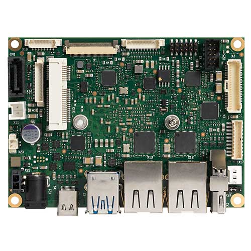
An SMT PCB is a printed circuit board specifically designed for Surface Mount Technology assembly, where electronic components are mounted directly onto copper pads on the PCB surface.
Compared with traditional through-hole technology (THT), SMT eliminates the need for component leads passing through drilled holes.
Common SMT components include:
- Resistors
- Capacitors
- Integrated circuits (ICs)
- BGA packages
- QFN components
- CSP devices
- Connectors
SMT PCBs are widely used in:
- Consumer electronics
- Automotive electronics
- Industrial control systems
- Medical equipment
- Communication devices
- IoT products
2. Why PCB Selection Is Important for SMT Assembly
The PCB acts as both:
- Electrical interconnection platform
- Mechanical support structure
An unsuitable PCB design may cause SMT problems such as:
- Poor solder joints
- Component misalignment
- Tombstoning defects
- Solder bridging
- Thermal stress failures
Therefore, PCB selection should consider the complete manufacturing process, including:
- PCB fabrication
- Component placement
- Solder paste printing
- Reflow soldering
- Inspection and testing
3. Key PCB Factors for SMT Applications
3.1 PCB Material Selection
The PCB substrate directly affects:
- Thermal performance
- Mechanical stability
- Electrical characteristics
- Long-term reliability
FR-4 PCB
FR-4 is the most commonly used SMT PCB material.
Advantages:
- Good mechanical strength
- Stable electrical performance
- Cost-effective
- Mature manufacturing process
Applications:
- Industrial electronics
- Consumer products
- General control boards
High-Tg FR-4 PCB
For applications involving higher temperatures, high-Tg materials are preferred.
Advantages:
- Better thermal resistance
- Improved dimensional stability
- Reduced PCB deformation during reflow
Applications:
- Automotive electronics
- Industrial equipment
- High-reliability products
High-Frequency PCB Materials
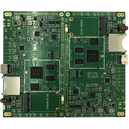
For SMT assemblies involving RF or high-speed signals, materials such as:
may be required.
Important parameters include:
- Dielectric constant (Dk)
- Dissipation factor (Df)
- Signal loss characteristics
Applications:
- RF modules
- Communication equipment
- Radar systems
4. PCB Surface Finish Selection for SMT
Surface finish directly affects solderability and assembly reliability.
Common SMT-compatible finishes include:
ENIG (Electroless Nickel Immersion Gold)
Advantages:
- Flat surface
- Excellent solderability
- Suitable for fine-pitch components
Applications:
- BGA
- QFN
- High-density PCB assemblies
ENEPIG
Advantages:
- Higher corrosion resistance
- Better wire bonding compatibility
- Improved reliability
Applications:
- High-reliability electronics
- Semiconductor-related products
HASL
Advantages:
- Cost-effective
- Good solderability
Limitations:
- Less suitable for very fine-pitch components due to surface unevenness
OSP
Advantages:
- Environmentally friendly
- Suitable for certain SMT applications
Considerations:
- Limited storage life
- Requires proper handling
5. PCB Design Considerations for SMT Components
5.1 Pad Design
Proper pad design is essential for reliable solder joints.
Engineers should consider:
- Component package type
- Pad dimensions
- Solder paste volume
- Manufacturing tolerances
Incorrect pad design may lead to:
- Insufficient solder
- Excess solder
- Solder bridging
5.2 Component Placement Design
SMT PCB layout should optimize:
- Component orientation
- Placement spacing
- Assembly sequence
Important considerations:
- Avoid placing sensitive components near heat sources
- Maintain sufficient clearance for inspection
- Consider rework requirements
5.3 Thermal Management
SMT components may generate significant heat.
Thermal design methods include:
- Thermal vias
- Copper areas
- Ground planes
- Heat dissipation structures
Poor thermal management may reduce:
- Component lifetime
- System reliability
5.4 PCB Thickness Selection
PCB thickness affects:
- Mechanical strength
- Reflow performance
- Assembly stability
Common PCB thicknesses include:
- 0.8mm
- 1.0mm
- 1.6mm
The selection depends on:
- Product structure
- Component requirements
- Mechanical constraints
6. SMT PCB Manufacturing Requirements
6.1 High Dimensional Accuracy
SMT assembly requires precise PCB dimensions.
Important parameters include:
- Board outline accuracy
- Hole position accuracy
- Pad registration
Poor accuracy may cause:
- Component placement errors
- Assembly defects
6.2 Solder Mask Quality
The solder mask affects:
- Solder control
- Pad definition
- Insulation reliability
Important requirements:
- Accurate opening size
- Good adhesion
- Stable thickness
6.3 Flatness Control
PCB flatness is critical for automated SMT equipment.
PCB warpage may cause:
- Poor contact during printing
- Component placement problems
- Uneven soldering
Especially important for:
- Large PCBs
- Thin PCBs
- BGA assemblies
7. SMT Assembly Process and PCB Requirements
7.1 Solder Paste Printing
The PCB must provide:
- Accurate pad geometry
- Good surface finish
- Proper stencil compatibility
7.2 Pick-and-Place Assembly
Automatic placement machines require:
- Accurate PCB positioning
- Reliable fiducial marks
- Stable board dimensions
7.3 Reflow Soldering
During reflow, the PCB experiences high temperatures.
Important PCB characteristics:
- Thermal stability
- Low moisture absorption
- Controlled expansion
Poor PCB quality may result in:
- Delamination
- Pad lifting
- Component defects
7.4 Inspection and Testing
Common SMT inspection methods include:
AOI (Automated Optical Inspection)
Detects:
- Missing components
- Incorrect placement
- Solder defects
X-Ray Inspection
Used for:
- BGA solder joints
- Hidden connections
- Internal defects
8. SMT PCB Design Challenges
8.1 High Component Density
Modern products require:
- Smaller packages
- More components
- Higher routing density
Solutions include:
- HDI PCB technology
- Microvias
- Advanced stack-up design
8.2 Mixed SMT and Through-Hole Assembly
Many products combine:
- SMT components
- THT connectors
- Mechanical components
Design challenges include:
- Assembly sequence
- Thermal profile control
- Clearance management
8.3 High-Speed Signal Requirements
Modern SMT PCBs often carry:
- High-speed digital signals
- RF signals
- Power switching signals
Design considerations include:
- Controlled impedance
- Signal return paths
- EMI suppression
9. How to Choose the Right PCB Manufacturer for SMT Projects
A qualified PCB supplier should provide:
Manufacturing Capability
- Multilayer PCB production
- HDI PCB capability
- Fine-pitch PCB manufacturing
- Controlled impedance capability
Assembly Capability
- SMT assembly
- BGA/QFN assembly
- Automated placement
- Reflow soldering
Engineering Support
- DFM analysis
- PCB stack-up optimization
- Component feasibility review
Quality Control
- AOI inspection
- X-ray inspection
- Electrical testing
- Reliability testing
10. Applications of SMT PCBs
Consumer Electronics
Examples:
- Smartphones
- Tablets
- Smart devices
Requirements:
- Compact size
- High component density
Automotive Electronics
Examples:
- Vehicle control units
- Sensor modules
Requirements:
- Thermal reliability
- Long-term stability
Medical Electronics
Examples:
- Monitoring devices
- Diagnostic equipment
Requirements:
- High reliability
- Stable performance
Industrial Electronics
Examples:
- Automation controllers
- Embedded systems
Requirements:
- Durability
- Continuous operation
Conclusion
Choosing the right PCB for SMT assembly requires consideration of multiple factors, including:
- PCB material
- Surface finish
- Pad design
- Thermal management
- Manufacturing accuracy
- Assembly compatibility
A properly designed SMT PCB can improve:
- Production yield
- Component reliability
- Electrical performance
- Product lifecycle
As electronic products continue moving toward smaller and smarter designs, advanced SMT PCB technologies will remain essential for achieving efficient and reliable electronic manufacturing.
