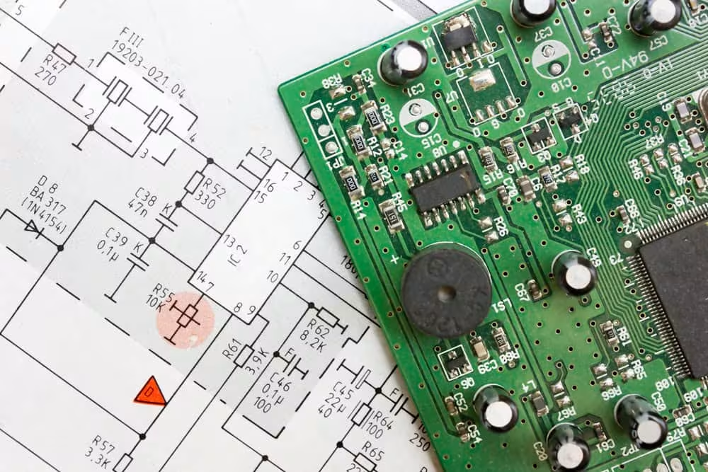
Printed Circuit Board (PCB) design is a critical step in the development of any electronic product. A well-designed PCB ensures reliability, performance, and manufacturability, while a poor design can lead to costly failures and delays. Below are five golden rules that every PCB designer should follow.
1. Prioritize Clear and Logical Layout
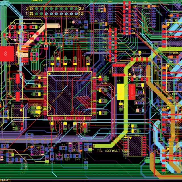
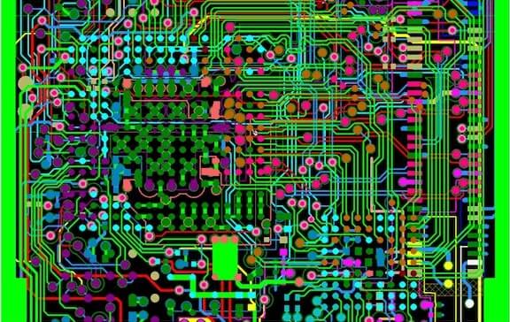
A clean and logical layout is the foundation of a successful PCB design. Components should be placed according to signal flow, grouping related parts together to minimize routing complexity.
Key tips:
- Place critical components first (MCUs, power modules)
- Keep signal paths short and direct
- Separate analog and digital circuits
2. Optimize Signal Integrity
Signal integrity is crucial, especially in high-speed designs. Poor routing can introduce noise, crosstalk, and signal distortion.
Key tips:
- Use proper trace width and spacing
- Avoid sharp angles (use 45° instead of 90°)
- Control impedance for high-speed signals
- Minimize via usage on critical traces
3. Ensure Proper Power Distribution
A stable power supply is essential for reliable circuit operation. Poor power design can lead to voltage drops and noise issues.
Key tips:
- Use wide traces or planes for power lines
- Add decoupling capacitors close to IC pins
- Implement proper grounding (star ground or ground plane)
4. Design for Manufacturability (DFM)
A good PCB design must be easy to manufacture. Ignoring manufacturing constraints can increase cost and reduce yield.
Key tips:
- Follow manufacturer design rules (trace width, spacing)
- Ensure proper solder mask clearance
- Avoid overly complex structures
- Standardize component footprints
5. Plan for Testing and Maintenance
Testing is essential to ensure product quality. Designing with testing in mind saves time during debugging and production.
Key tips:
- Add test points for critical signals
- Use clear labeling (silkscreen)
- Allow space for probes and inspection
- Consider modular design for easier repair
Conclusion
Following these five golden rules can significantly improve PCB design quality, reduce errors, and accelerate time-to-market. Whether you are designing simple circuits or complex multilayer boards, these principles remain essential.
