HomeCategory

PCB Assembly (PCBA) Services | Turnkey Solutions - KKPCB

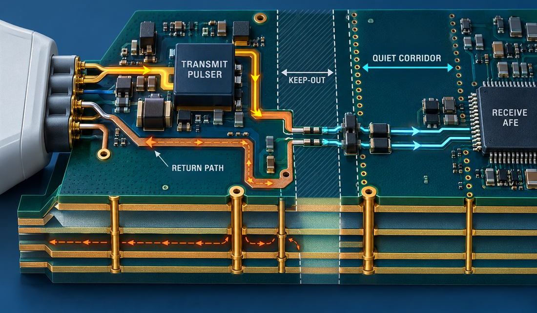
How to Keep a High-Voltage Pulser from Polluting an Ultrasound PCB Receive Path

Ultrasound PCB partitioning becomes difficult when the transmit pulser and the receive AFE share a small probe-side area. During a transmit event, a short high-voltage pulse can create a large local current loop, while the receive channel is trying to preserve a much smaller echo signal. If the board treats those two functions as ordinary...
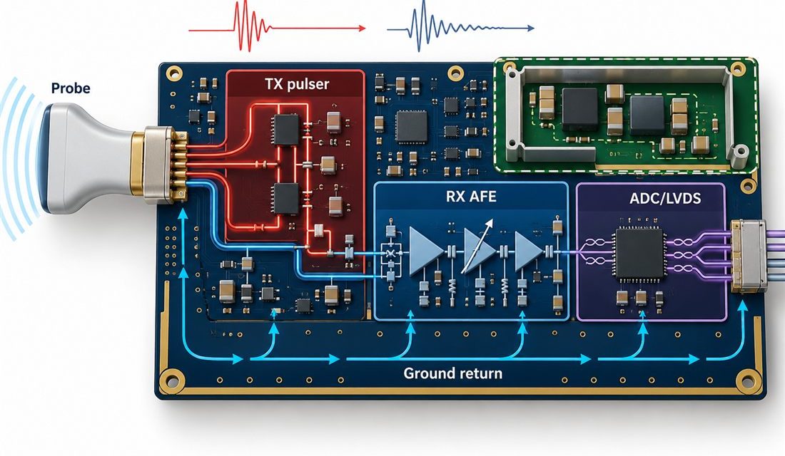
When Ultrasound Echoes Become Layout Noise: A Low-Noise Ultrasound PCB Release Plan

Ultrasound PCB design fails in a very specific way: the image can look acceptable on a bench and then lose contrast when transmit voltage, receive gain, clock activity, and patient-interface cabling are present at the same time. The difficult part is not choosing an expensive AFE; it is preserving the receive signal while the board...

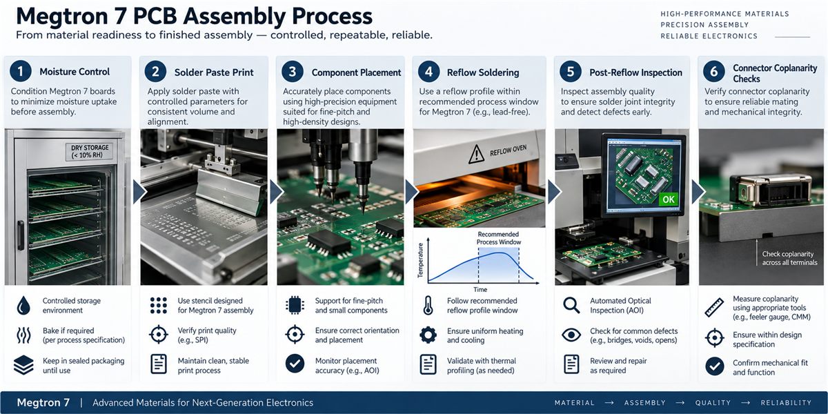
Megtron 7 PCB Assembly: Moisture, Reflow, and Coplanarity Controls for High-Speed Modules

A high-speed board can pass fabrication inspection and still lose performance during assembly. Moisture exposure, an unsuitable reflow window, connector coplanarity, or residue under a shield can change the mechanical position of a launch and weaken a controlled return path. A production-ready Megtron 7 PCB connects material handling to RF and signal-integrity requirements. Table of...

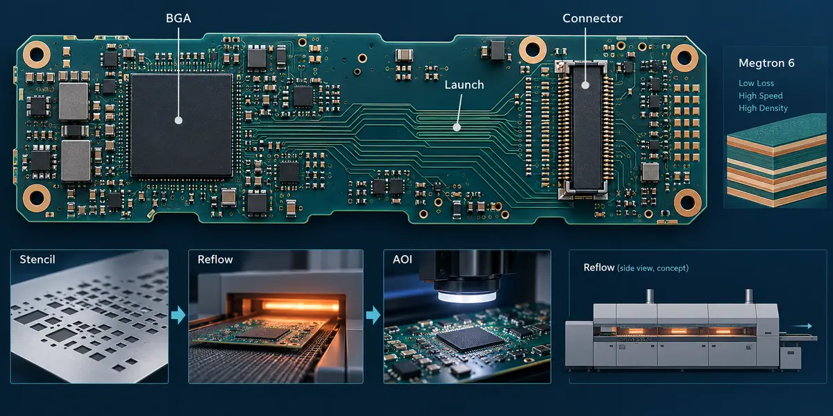
Megtron 6 PCB Assembly: A Reflow and Connector-Launch Plan for High-Speed Modules

The Megtron 6 PCB connector launch remains the shared datum for SI and assembly inspection. The production Megtron 6 PCB callout should travel with the reflow and inspection package. A connector change on a Megtron 6 PCB is an electrical and assembly change, not only a mechanical edit. For the release team, a Megtron 6...

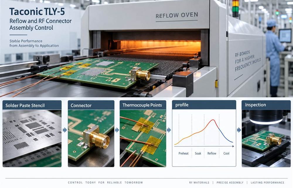
Taconic TLY-5 PCB Assembly Window: Reflow and Connector Workmanship for RF Builds

Table of Contents Define the RF assembly window before quoting Protect the connector launch through reflow Inspect solder and cleanliness without disturbing RF geometry Control rework and release evidence RF boards can meet bare-board inspection and still miss the project target after assembly. A connector pin may pull a launch pad, solder mask can creep...

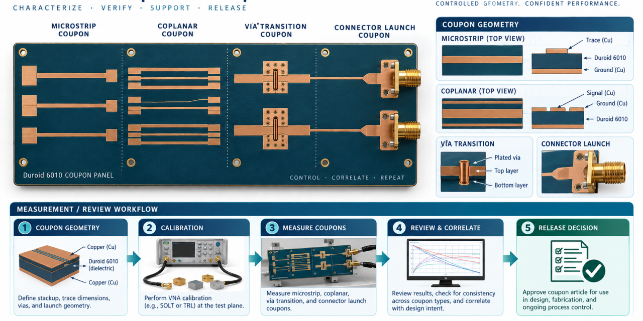
Duroid 6010 PCB Impedance Coupons: 7 Critical Controls for Production Release

Table of Contents Why coupon design must follow the RF path Seven controls for defensible coupon evidence Geometry, calibration, and correlation Release package and handoff Coupon checklist A Duroid 6010 PCB impedance coupon is useful only when its geometry, construction, fixture, and acceptance method represent the product feature being released. The project pain point is...

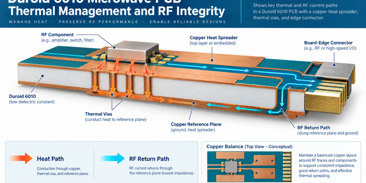
Duroid 6010 PCB Thermal Management: 7 Critical Controls for Stable RF Power

Table of Contents Why thermal and RF paths interact Seven controls for stable power handling Heat path and copper balance Qualification and release evidence Engineering checklist A Duroid 6010 PCB can support compact microwave routing, but RF power and thermal design must be released together. The project pain point is the interaction between copper spreading,...

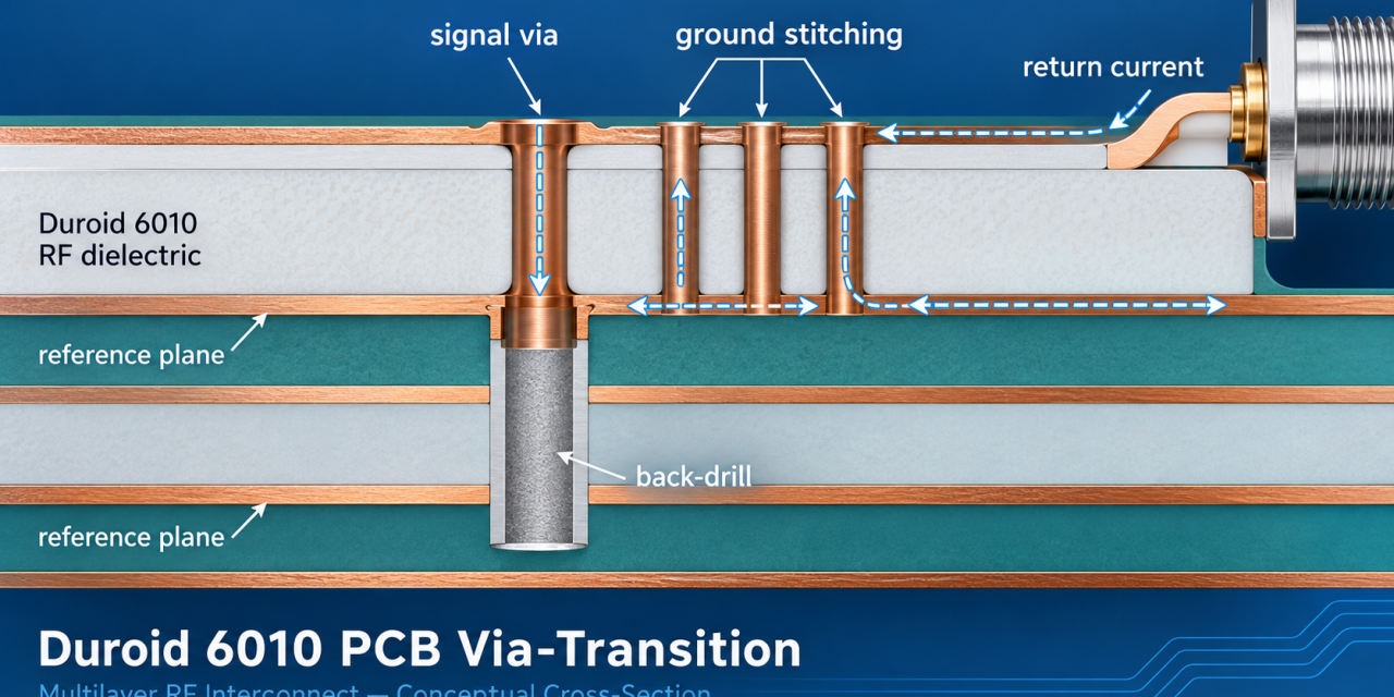
Duroid 6010 PCB Via Transition: 7 Critical Controls for Stable RF Interconnects

Table of Contents Why via transitions become the RF bottleneck Seven controls for a stable interconnect Return path and back-drill Launch and inspection evidence Release checklist A Duroid 6010 PCB via transition can dominate microwave performance when the signal changes layers, connects to a board-edge launch, or crosses a split reference plane. The project pain...

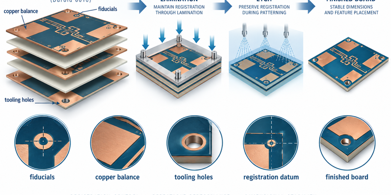
Duroid 6010 PCB Dimensional Stability: 7 Critical Controls for RF Registration

Table of Contents Why dimensional drift affects RF builds Seven controls for registration stability Panel balance and datums Inspection and release evidence Project checklist A Duroid 6010 PCB can be electrically well designed and still miss the project’s RF margin when layer-to-layer registration, copper balance, or board-edge datums drift through lamination and etch. The real...