
The Megtron 6 PCB connector launch remains the shared datum for SI and assembly inspection.
The production Megtron 6 PCB callout should travel with the reflow and inspection package.
A connector change on a Megtron 6 PCB is an electrical and assembly change, not only a mechanical edit.
For the release team, a Megtron 6 PCB handoff should name the same datum in fabrication and assembly.
Megtron 6 PCB assembly programs can lose high-speed margin after fabrication if reflow, connector loading, and inspection are treated as separate workstreams. The laminate may be selected for low dielectric loss, but the assembled module still depends on solder-mask clearances, component coplanarity, launch geometry, thermal gradients, and cleaning controls. This article gives manufacturing engineers and project managers a practical release path for dense high-speed modules.
Table of Contents
- Reflow and material interaction
- Connector launch controls
- Inspection and prototype evidence
- Production release checklist
Connect the laminate decision to the assembly process
A Megtron 6 PCB stackup is designed around a finished dielectric, copper distribution, and reference-plane system. Assembly adds thermal exposure, solder-mask definition, paste deposition, component pressure, and mechanical support. If the board house and assembler use different datums, a connector pad or RF launch can shift relative to the controlled-impedance path even though the bare-board drawing is correct.
Panasonic MEGTRON 6 family data should be read for the exact grade and construction, including typical Tg, Td, CTE, Dk, and Df test methods. Those typical values help establish a design window; they do not replace a released reflow profile or a finished-board inspection plan.
Plan the reflow path around high-speed geometry
Protect the reference plane and surface finish
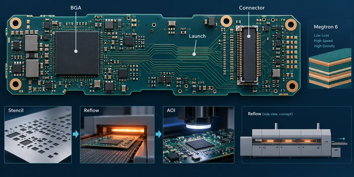
Large copper planes, thermal spokes, and connector ground fields change how heat spreads during reflow. Balance the panel where possible and keep solder-mask expansion consistent around differential pads. Avoid placing a plane void directly under a launch unless the electrical model and assembly drawing both approve it. The PCB assembly review should compare the paste aperture, pad stack, mask opening, and adjacent return vias as one feature.
The chosen surface finish must also match the assembly window. Plating thickness, pad flatness, and solderability affect connector coplanarity and the repeatability of fine-pitch joints. A Megtron 6 PCB module should document the finish, storage or conditioning limits, and the inspection method before the first production build.
Control connector launches and transitions after assembly
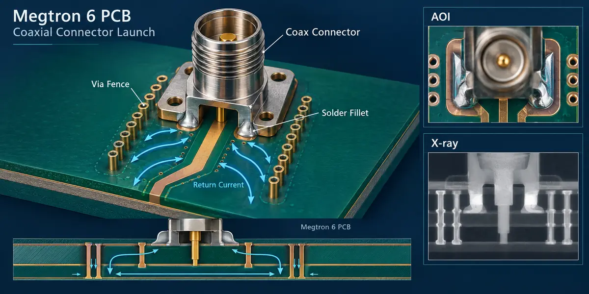
Connector launches are short three-dimensional structures. Pad length, antipad diameter, solder-mask clearance, connector ground tabs, and via-fence spacing determine whether the RF return path remains continuous. Keep the launch geometry consistent between the bare board, assembly drawing, and mechanical model. The PCB layout review should show the signal pad, reference plane, return vias, keep-out, and component body in the same datum view.
For high-density modules, do not let a late connector replacement move the launch or change the ground-tab pattern without rechecking the stackup. The high-speed PCB manufacturing package should specify drill tolerance, plating range, copper balance, and the cross-section request used to verify the transition.
Use inspection evidence that matches the risk
Visual inspection alone cannot confirm a high-speed launch. Combine solder-joint inspection, connector coplanarity, cross-section evidence, and dimensional checks around the critical datum. If a via transition or ground fence is important to the channel, make it visible in the inspection drawing and coupon plan. The Megtron 6 materials reference confirms the selected family, while the finished product evidence confirms whether the process held the intended construction.
For prototypes, PCB prototype assembly can expose stencil, reflow, connector, and cleaning risks before tooling is fixed. Treat prototype findings as inputs to the production release, not as proof that every future panel will behave identically. A process change, connector substitution, or new panel array should reopen the inspection and thermal review.
Production release checklist
- Material grade, finished dielectric, copper range, and surface finish defined in one revision.
- Reflow profile, board support, component keep-outs, and mask expansion approved for the critical launch.
- Connector pad, antipad, return-via, ground-tab, and mechanical datum shown together.
- Inspection plan includes solder joints, coplanarity, cross-section, registration, and launch features.
- Prototype findings and supplier changes recorded in engineering change control.
- Assembly and fabrication teams use the same stackup, datum, and coupon terminology.
For a project manager, a Megtron 6 PCB release is complete only when the SI drawing, fabrication notes, and assembly inspection plan agree. The final Megtron 6 PCB production package should make the connector launch and reflow assumptions auditable.
Sources: Panasonic Industrial Devices MEGTRON 6 family and R-5775/R-5670 technical data; supporting high-speed assembly and RF transition guidance from Analog Devices and Qorvo application material; KKPCB verified pages for manufacturing, layout, assembly, prototype assembly, and MEGTRON 6 material capability. Values are typical or design-reference values unless a released drawing defines the acceptance limit.
