
RF boards can meet bare-board inspection and still miss the project target after assembly. A connector pin may pull a launch pad, solder mask can creep into an exposed field, or a shield installation can change the local return path. A Taconic TLY-5 PCB assembly plan should define the reflow, cleaning, inspection, and rework window before the first lot is scheduled. That is especially important when the board feeds a Ku-band radio, GNSS receiver, radar sensor, or compact beamforming module.
Define the RF assembly window before quoting
Start with the interface that cannot be repaired by software: connector launch, antenna pad, filter footprint, or RF shield land. For a Taconic TLY-5 PCB, freeze the stackup and exposed-copper condition, then state the paste family, stencil opening, component placement tolerance, and cleaning route. The material’s typical electrical data is only the RF starting point; solder fillet shape, mask opening, and connector seating determine the finished interface.
Create a solder paste and assembly risk table with three columns: the RF feature, the process variable, and the evidence required. A project manager can then see whether a proposed supplier change affects phase, loss, or workmanship. Do not wait until a connector is already on the line to discover that the inspection camera cannot see the inner ground pins.
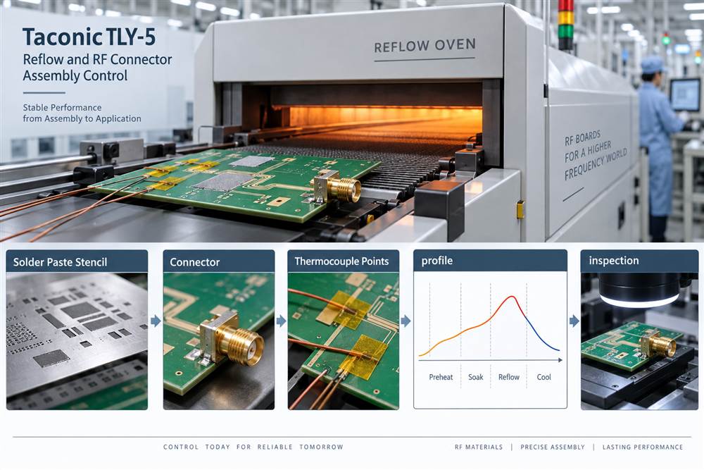
Protect the connector launch through reflow
The launch footprint should be released as an RF feature, not only as a component land pattern. A Taconic TLY-5 PCB connector launch needs finished pad dimensions, ground-pin land pattern, mask opening, keep-out, and the reference plane below it. Use controlled-impedance PCB notes to show where solder mask is allowed and where the RF field must remain predictable.
During reflow, coplanarity, paste volume, and board support influence whether the connector remains square. A connector that tilts by a small amount can stress the launch or leave one ground pin partially wetted. Define a support strategy for thin panels, identify the fiducials used for placement, and keep the launch away from depanelization strain. If a shield is installed in a second pass, confirm that the second thermal cycle does not exceed the approved assembly window.
Process controls worth freezing
- Paste print inspection at the RF launch and connector ground pins.
- Profile limits at the board surface, not only at the oven recipe.
- Support tooling that avoids bending the antenna edge or connector region.
- Placement and coplanarity checks for RF connectors and shields.
Inspect solder and cleanliness without disturbing RF geometry
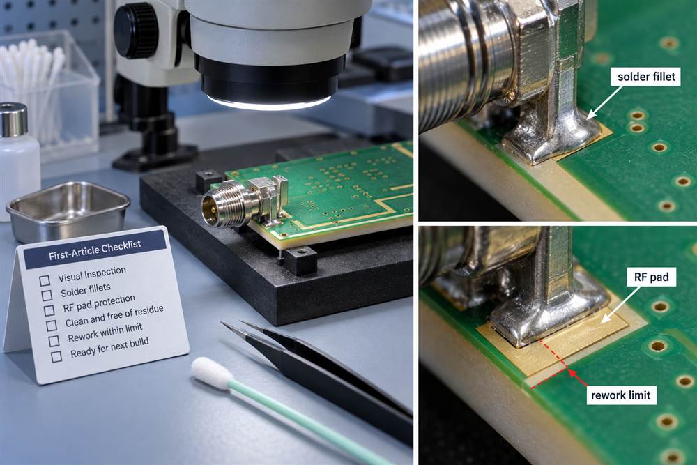
The PCB assembly inspection plan should combine optical views, X-ray where hidden joints require it, and a mechanical check of connector seating. Identify the solder fillet, pad edge, via fence, and shield land in the same inspection view. A generic “pass” photo does not prove that an RF launch is centered or that paste has not bridged a ground gap.
Cleaning is an RF concern when residue changes contact, traps moisture, or enters a connector. State whether the process is no-clean, aqueous, or solvent-based; then protect the laminate, shield, and connector surfaces accordingly. For a TLY-5 build, the team should also document dry-bake or storage limits when the product’s field environment makes moisture a concern. These are process controls, not claims of a customer test result.
Control rework and release evidence
When an RF connector fails inspection, define the rework limit before touching the board. Record the number of heat cycles, the tool, the flux or paste used, the pad condition, and the final coplanarity check. Rework is not automatically harmless because the laminate survives the oven; pad adhesion, mask edge, and launch geometry can still move.
During PCB manufacturing handoff, correlate the assembly drawing with the bare-board stackup, via fence, and finish. A finish change can alter solder wetting and connector contact; a mask change can alter the RF field. If the assembled board uses a Taconic TLY-5 PCB launch, retain the same drawing revision through fabrication, assembly, and test.
For program release, use a RF assembly traveler that lists the approved profile, inspection points, cleaning method, rework gate, and photo evidence. The traveler should distinguish target values from measured observations and identify the lot, operator, and board revision.
RF assembly release checklist
- Freeze the connector, pad, mask, reference-plane, and shield geometry.
- Approve paste, stencil, support, profile, and placement conditions.
- Inspect hidden joints, connector seating, solder fillets, and cleanliness.
- Set a documented rework limit and record every rework cycle.
- Keep assembly, fabrication, and RF test on one controlled revision.
The result is a Taconic TLY-5 PCB assembly process that protects the same electrical intent created in layout. When the process window is explicit, procurement can compare suppliers on evidence instead of promises, and engineering can investigate a failure without guessing which thermal or mechanical change occurred.
For procurement, the Taconic TLY-5 PCB assembly traveler should preserve the Taconic TLY-5 PCB launch drawing and the Taconic TLY-5 PCB rework limit. Keep the Taconic TLY-5 PCB inspection evidence with the lot record so a connector change is visible.
Review the Taconic TLY-5 PCB finish, the Taconic TLY-5 PCB connector seating, and the Taconic TLY-5 PCB cleaning route together before release.
Sources: AGC public TLY-5 material data; Analog Devices and Qorvo RF assembly and layout practices; connector and RF front-end workmanship guidance; KKPCB fabrication and PCBA release methods reviewed for this article.
