
PTFE assemblies fail in ways that are easy to misclassify. A void under a thermal pad can look like a material problem; a connector that is slightly tilted can look like a launch problem; residue near a high-impedance node can look like a dielectric shift. A PTFE PCB program needs an assembly plan that protects the RF geometry while acknowledging that PTFE and ceramic-filled systems may respond differently to heat, pressure, and cleaning than standard FR-4.
Define the assembly window around the RF features
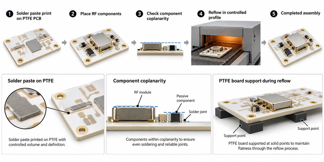
Start with the component mix and the board’s mechanical support. The PTFE PCB panel should show fiducials, tooling support, carrier or pallet requirements, and any edge area that must remain flat for a connector. Keep the RF launch, antenna, and high-impedance pads away from paste apertures or adhesive features that can migrate during reflow.
Set a profile window based on the material and component limits, then confirm the actual oven profile on the assembled panel. The RF PCB assembly note should define ramp, soak, peak, time above liquidus, cooling rate, and the locations used for thermocouples. Do not copy a profile from a conventional laminate without checking the material supplier’s limits.
Stencil design is part of RF design when solder thickness changes pad height or connector coplanarity. Use aperture reductions and local step-downs only after confirming that the paste volume still supports the thermal and mechanical requirement.
Control cleaning and moisture risk
Select the cleaning chemistry, brush or spray energy, and drying method with the material stack and component seals in mind. A PTFE PCB can have low bulk moisture uptake while flux residue or trapped water remains at a connector, shield, or via field. The controlled impedance process window should state the wash temperature, rinse quality, dry time, and inspection point.
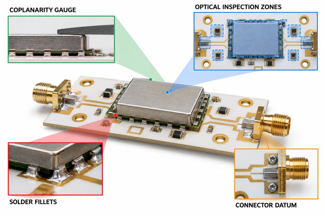
Inspect the RF region for residue, solder splashes, and mask damage before electrical test. The most useful evidence is a defined visual standard tied to the location and severity, not a general statement that the board was cleaned.
If the product will see humidity or condensation, add a controlled bake or storage rule only when the assembly and component suppliers support it. Record the board exposure time rather than assuming an unlimited floor life.
Verify coplanarity and RF interfaces
Measure connector and shield coplanarity against the mechanical drawing and inspect the solder joint where the RF reference plane enters the board. The thermal management assembly handoff should identify which dimensions are measured before and after reflow.
Use a functional or network test that represents the product interface, but keep the interpretation separate from the assembly evidence. A clean visual inspection does not prove insertion loss, and a passing RF test does not prove long-term solder reliability.
For the first build, freeze a photo standard, profile record, inspection report, and sample traceability. That package makes process changes easier to evaluate and prevents a rework decision from becoming an undocumented RF change.
PTFE PCB assembly quality comes from controlling the thermal, chemical, and mechanical interfaces together. Give the assembler a defined process window and give the RF team evidence tied to the actual connector and line geometry.
Implementation note for this assembly and reflow reliability review: keep the engineering assumption visible at the point where it affects a drawing, a supplier quote, or an inspection record. Ask the design owner to identify the reference plane, interface datum, and acceptance method before the release is frozen. Ask manufacturing to return the proposed stack, panel, and process window rather than a generic capability statement. Ask assembly to identify the profile, cleaning, and support conditions that could move the RF or thermal result. This simple handoff prevents a typical material value from being mistaken for a guaranteed product result and gives the project team a clear action when an ECO changes the physical boundary.
Release note: keep the PTFE PCB assembly profile, cleaning method, and support condition in the build record so RF performance is not separated from solder-process evidence.
Sources: Panasonic MEGTRON technical material guidance; Rogers and Taconic high-frequency material data sheets where relevant; CeramTec ceramic substrate data; Analog Devices RF and mixed-signal layout guidance. Numerical values are treated as typical supplier values or engineering targets unless the released drawing defines a measured acceptance value.
Release note: confirm the PTFE PCB construction before the next ECO.
Release note: confirm the PTFE PCB construction before the next ECO.
Release note: confirm the PCB manufacturing evidence before approval.
Release note: confirm the PCB assembly evidence before approval.
