HomeTag

IoT Sensor PCB - KKPCB

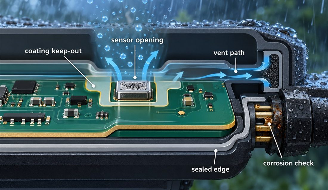
Why an IoT Sensor PCB Drifts After Coating and Humidity Exposure

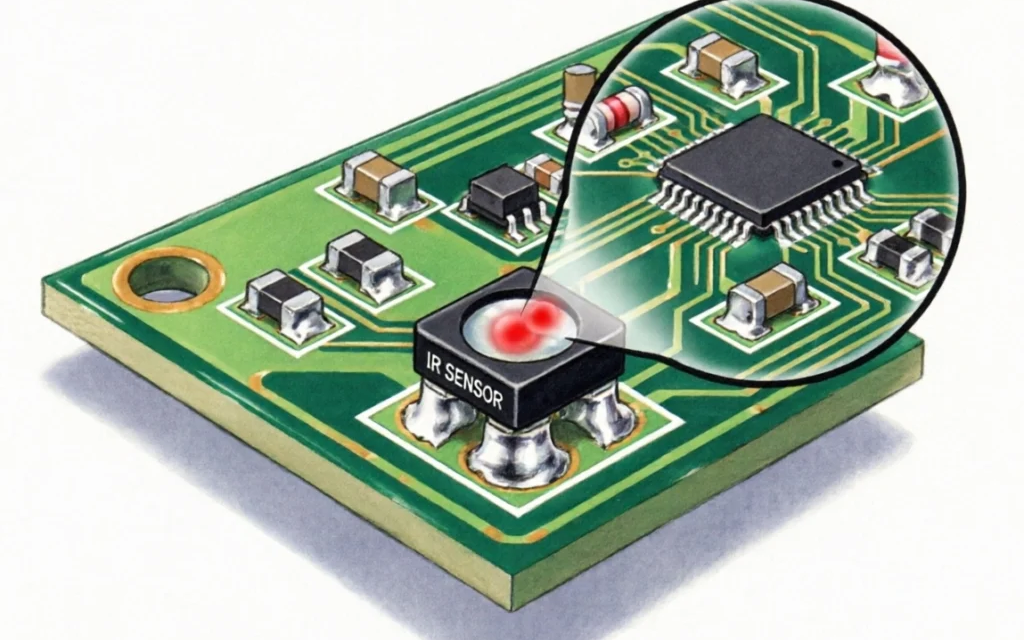
Table of Contents Why environment becomes a signal problem Design coating and sensor keep-outs together Build a repeatable qualification path Release evidence for field service An environmental sensor can be electrically correct on the bench and still drift after weeks of humidity, condensation, cleaning, and temperature cycling. The enclosure, coating, vent, connector, and copper pattern...
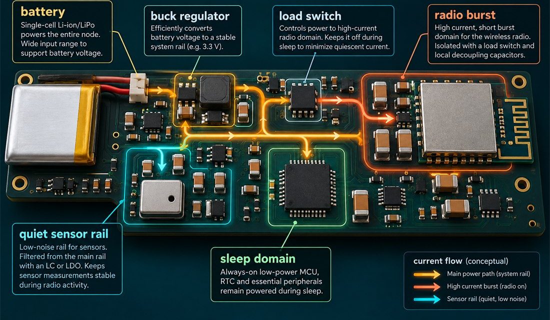
How to Release an IoT Sensor PCB for Repeatable Volume Calibration

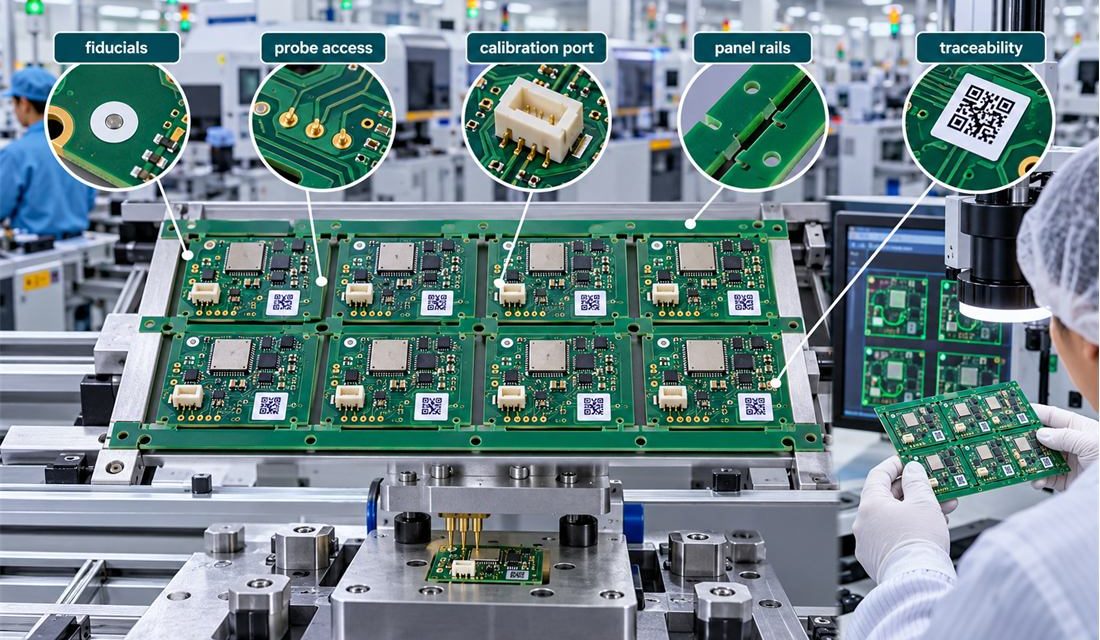
Table of Contents Why a stable design still fails at volume Design the panel for inspection Make calibration repeatable Control revision and supplier changes A prototype can produce excellent sensor readings and still become a difficult product to build. The problems appear when a small IoT Sensor PCB moves into panels, fixtures, alternate components, and...

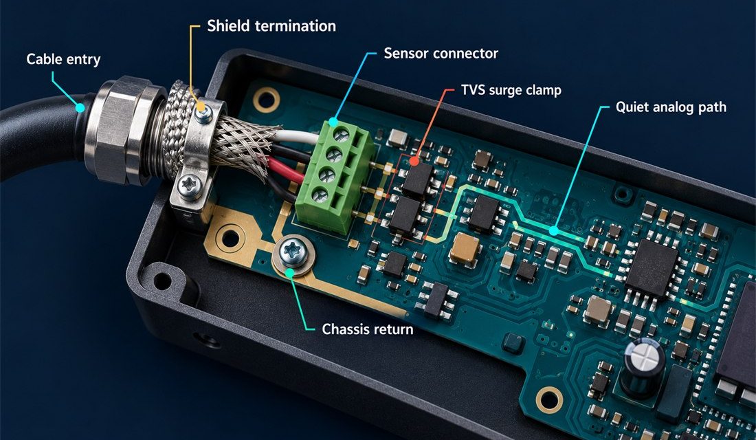
The Quiet Return Path an IoT Sensor PCB Needs for Trustworthy Readings

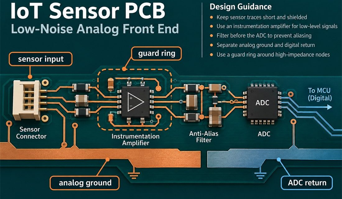
Table of Contents Why a stable sensor gives unstable numbers Build the analog path before the digital path Treat ground and references as measurement structures Keep accuracy through assembly Release a repeatable measurement board An IoT Sensor PCB can use a high-quality sensor and still report noisy or drifting values when the board couples digital...

High Frequency Sensor PCB: Advanced RF PCB Solutions for Precision Sensing and Real-Time Signal Processing

The Growing Demand for High Frequency Sensor PCB Technology Modern sensing technologies are rapidly evolving toward: Higher operating frequencies Real-time signal acquisition Faster wireless communication Compact sensor integration Intelligent data processing Applications such as: Automotive radar systems Industrial IoT sensors Aerospace monitoring equipment Medical imaging systems Smart manufacturing platforms require highly reliable High Frequency Sensor...

High Frequency Sensor PCB – Precision Low-Loss PCB for RF and Microwave Sensing Applications

What Is a High Frequency Sensor PCB? A High Frequency Sensor PCB is a specialized printed circuit board engineered to support sensors operating in RF and microwave frequency ranges. These boards are designed to maintain signal accuracy, minimize transmission loss, and ensure stable performance under demanding environmental conditions. High-frequency sensors are widely used in: Radar...

Impedance Controlled PCB – High Precision PCB for High Speed Signal Integrity

What Is an Impedance Controlled PCB? An Impedance Controlled PCB is a printed circuit board designed to maintain precise characteristic impedance along signal traces. This is critical for high speed digital circuits, RF communication, and microwave systems, where mismatched impedance can cause: Signal reflection Crosstalk Data errors Timing skew Impedance control ensures reliable signal integrity...

High Frequency Sensor PCB – Low Loss PCB for RF and IoT Sensor Applications

What Is a High Frequency Sensor PCB? A High Frequency Sensor PCB is a specialized printed circuit board designed for RF, microwave, and IoT sensor modules. These PCBs enable accurate data acquisition and signal processing for applications such as: Radar sensors Ultrasonic sensors LiDAR modules High speed IoT devices Wearable sensor systems High Frequency Sensor...

IoT Sensor PCB Engineering: High-Performance Design and Manufacturing for the Connected Future

The Internet of Things (IoT) is reshaping industries by connecting intelligent devices, collecting real-time data, and enabling automated decision-making. Behind every connected device is a critical hardware foundation — the IoT Sensor PCB. From industrial monitoring systems and smart home products to wearable devices and healthcare equipment, IoT sensor PCBs provide the platform for: sensor...