
Table of Contents
An environmental sensor can be electrically correct on the bench and still drift after weeks of humidity, condensation, cleaning, and temperature cycling. The enclosure, coating, vent, connector, and copper pattern all influence the reading. A robust IoT Sensor PCB therefore treats environmental protection as a measurement-design problem, not a final spray operation. The project team needs to know where moisture may enter, which surfaces must remain exposed, and how a service technician can prove that the sensor opening and reference path are still valid.
Why environment becomes a signal problem
Humidity changes leakage, dielectric behavior, connector contact resistance, and the chemistry around a sensor opening. A thin film across a high-impedance node can create a bias that looks like sensor drift. A trapped pocket near a vent can delay equilibration and make two otherwise identical units respond at different speeds. The first IoT Sensor PCB review should map the sensing surface, guard copper, analog reference, coating boundary, vent route, and drain path.
Do not begin with a generic “conformal coat all exposed copper” instruction. Define what the sensor needs to contact: air, gas, pressure, or a calibrated membrane. Then define what the circuit needs protected: high-impedance traces, fine-pitch packages, exposed vias, and connector transitions. A sensor keep-out drawing gives manufacturing a measurable boundary instead of a visual guess.
Temperature cycling adds a mechanical dimension to an IoT Sensor PCB. The laminate, solder joints, enclosure, coating, and sensor package expand at different rates. If the coating bridges a flexible connector or fills a vent path, the board can pass an initial electrical test and fail after repeated transitions. For a released IoT Sensor PCB, freeze the material system and assembly sequence before the team tunes calibration coefficients.
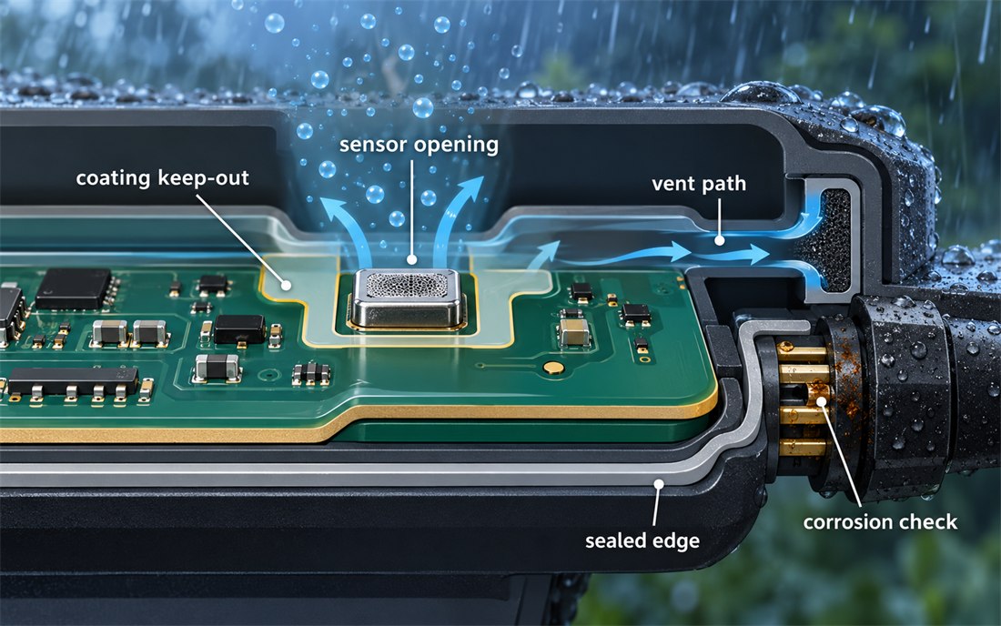
This conceptual drawing shows a sensor opening, coating keep-out, vent route, sealed edge, and corrosion inspection area. It is a design explanation, not a field photograph. Use a moisture-path review to align the board finish, enclosure seal, and sensor response requirement before production release.
Design coating and sensor keep-outs together
Masking is part of the PCB definition. Specify the mask material, registration allowance, removal method, and visual acceptance at the sensor opening, connector, test pads, and mechanical datum. A coating-mask fixture should hold the board without touching the sensing surface or loading a delicate connector. The work instruction should show orientation and the order of masking, coating, cure, inspection, and mask removal.
Surface finish and cleanliness also matter. Ionic residues under a coating can absorb moisture and create a leakage path that is difficult to reproduce on a dry bench. Define cleaning chemistry, drying time, handling gloves, and the inspection method with the assembly supplier. The cleanliness checkpoint should be tied to the actual high-impedance nets, not copied from a generic assembly checklist.
Keep the sensor reference quiet while the protection structure remains mechanically strong. Guard traces, slots, and copper clearances should be reviewed with the enclosure and airflow path. A guard-ring detail can reduce surface leakage, but it cannot compensate for a contaminated connector or a vent blocked by adhesive.
Build a repeatable qualification path
Qualification should separate functional drift from environmental recovery. Establish a reference fixture, a known stimulus, a stable supply, and a controlled wait time before each reading. A calibration-reference fixture must hold the board, sensor port, and cable consistently so operators do not introduce a different angle or contact force each time.
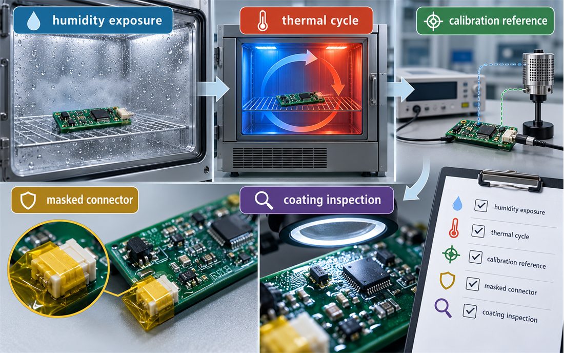
The second conceptual image shows humidity exposure, thermal cycling, a calibration reference, a masked connector, and coating inspection. It is a workflow illustration, not a customer test report. Use environmental release evidence to record the board revision, coating lot, fixture revision, sensor lot, and recovery observation at each stage.
Run baseline readings before exposure, then record the first stable value, the response time, the recovery path, and any visual change. Separate a reversible moisture effect from a permanent corrosion or delamination issue. A drift-trend worksheet helps the engineering team compare units without hiding the time history behind one pass/fail number.
Release evidence for field service
Field service needs a way to identify whether a sensor problem is environmental, electrical, or mechanical. Include the coating boundary, sensor opening dimensions, connector mask, approved cleaning method, calibration fixture, and service inspection photographs in the release package. A service-inspection map should point to physical features that a technician can actually see.
- Freeze the sensor opening, vent, guard, and coating keep-out in the drawing.
- Control cleaning, drying, masking, coating, and cure as one assembly route.
- Record baseline, exposure, recovery, and visual inspection evidence in a production traveler by board revision.
- Repeat the qualification path after enclosure, coating, sensor, or adhesive changes.
- Keep service limits separate from design targets so field teams know when to return a board.
A reliable IoT Sensor PCB is not defined by a coating brand alone. It is defined by a controlled boundary between the sensing surface and the protected electronics, supported by a fixture, an inspection method, and evidence that survives a real environment. That boundary gives engineers a practical way to protect accuracy without making the sensor blind.
Keep the service boundary visible
The field team needs a practical way to separate sensor drift from board contamination. For an IoT Sensor PCB, keep the sensor opening, coating edge, connector mask, and calibration reference visible in the service drawing. The IoT Sensor PCB record should identify the environmental exposure, board revision, coating lot, and fixture used for the last approved reading.
When a housing seal, adhesive, or sensor vendor changes, do not change the calibration limit first. Re-run the moisture path, inspect the masked connector, and compare recovery behavior with the approved reference. This makes the IoT Sensor PCB easier to support because the team can explain whether a shift is caused by the environment, the assembly route, or a genuine circuit change.
Sources: Analog Devices sensor-interface and mixed-signal layout guidance; Würth Elektronik assembly, cleaning, and coating notes; Qorvo environmental RF integration references; sensor and coating supplier technical data. Values above are engineering practices or design targets, not customer measurements.
