
Table of Contents
A prototype can produce excellent sensor readings and still become a difficult product to build. The problems appear when a small IoT Sensor PCB moves into panels, fixtures, alternate components, and a production line that must identify every unit. Probe access disappears under a support rail, a calibration connector is hard to seat, or a supplier change shifts the analog reference enough to create a false field trend. The solution is to release the board as a manufacturing system, not as a drawing with components. Add a process-window review before the first volume run.
Why a stable design still fails at volume
Production variation is rarely one dramatic defect. It is usually the accumulation of stencil alignment, paste volume, connector seating, cleaning residue, component tolerance, firmware revision, and fixture contact. A volume-ready IoT Sensor PCB starts with a list of characteristics that can change the measurement: sensor placement, reference routing, ground return, regulator output, test-pad access, and the mechanical datum used by the enclosure.
Separate design targets from acceptance limits. A target may describe the intended sensor offset or settling behavior; an acceptance limit defines what the line can verify. A release-characteristic matrix should identify the owner, method, fixture, sampling plan, and reaction when a value is outside the agreed range. Without that matrix, every supplier review becomes a new interpretation of the same drawing.
Alternates need the same discipline. A regulator with a similar name may have different enable timing or thermal behavior. A connector with the same pitch may change contact force or shield continuity. Lock the parameters that matter to the sensor, and route each proposed alternate through a documented IoT Sensor PCB engineering review before the first article.
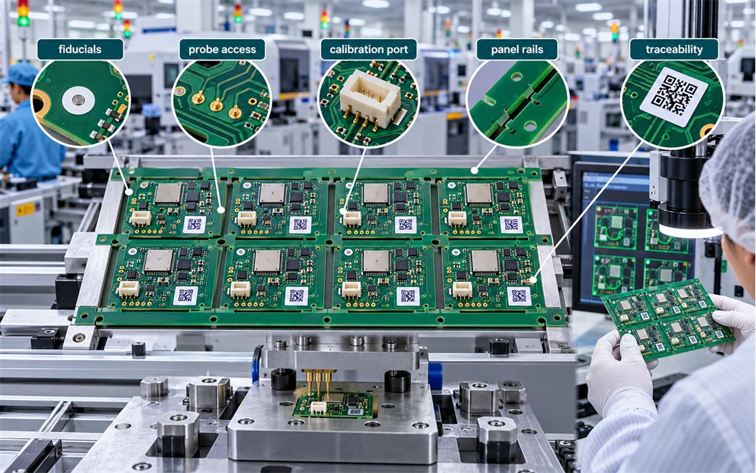
This conceptual manufacturing image highlights fiducials, probe access, calibration port, panel rails, and traceability. It is an explanatory graphic, not a customer production photograph. For a released IoT Sensor PCB, the panel drawing, support points, and test-pad map should be reviewed before tooling is frozen.
Design the panel for inspection
Panelization changes the mechanical and electrical environment of the unit. Breakaway tabs, rails, copper balance, and routing direction can bend a sensor opening or stress a connector. Keep the sensing area away from the most aggressive depanelization features, give the fixture a stable datum, and expose test points where a probe can reach them without touching a fragile package. A panel-support drawing makes those choices visible to the assembly team.
Fiducials are not decoration. Their size, solder-mask clearance, and relation to the panel rails influence placement accuracy. If the board uses a calibration connector or optical sensor, include its actual keep-out in the placement and inspection documents. A first-article inspection map should identify connector coplanarity, solder coverage, orientation, and any feature that affects the sensor datum.
Plan rework before the first build. Define which components can be replaced, how the board is supported, where heat may be applied, and how calibration is repeated after repair. A controlled rework boundary prevents a technician from disturbing a sensor opening or a reference component while solving an unrelated solder defect.
Make calibration repeatable
Calibration is a measurement process with mechanical tolerances. The fixture must locate the board, expose the sensor to a known stimulus, connect power and communications, and record the board revision. A calibration-fixture datum should be defined on the drawing, not left to an operator’s hand. Use a golden sample to check the fixture at the start of a shift and after any maintenance.
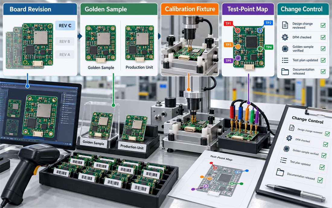
The second conceptual image shows board revision control, a golden sample, calibration fixture, test-point map, and change-control checks. It contains no measured values. Use a calibration-record format that stores stimulus, firmware build, board serial, fixture serial, operator, and disposition together.
When readings move, compare the fixture before changing the board. Check probe pressure, connector seating, supply drop, firmware, sensor lot, and ambient condition in that order. A material-and-process log can reveal that a coating, cleaning step, or solder profile changed at the same time as the calibration trend.
Control revision and supplier changes
Every released unit should be traceable to the data that made its reading acceptable. Open a supplier-change ticket for every approved alternate. Put the board revision, firmware version, sensor lot, fixture revision, and disposition in the manufacturing record. A traceability label plan should survive panel separation and remain readable after enclosure assembly.
- Freeze panel rails, fiducials, support points, and probe access before tooling.
- Define calibration datum, golden sample, stimulus, and record format.
- Inspect connector seating, sensor keep-outs, solder coverage, and polarity.
- Route alternates and process changes through DFM and engineering review.
- Repeat calibration after rework, firmware changes, coating changes, or fixture maintenance.
A production-ready IoT Sensor PCB gives engineering, purchasing, and manufacturing the same definition of “good.” That shared definition reduces false rejects, prevents untraceable field units, and makes a supplier change a controlled decision rather than a surprise discovered after shipment.
Make the handoff auditable
Before shipment, the IoT Sensor PCB release should let a second team reproduce the calibration decision without asking the designer to interpret private notes. Package the panel drawing, approved BOM alternates, fixture datum, golden-sample ID, probe map, firmware build, and reaction plan together. The IoT Sensor PCB serial record should show which fixture and operator produced the reading, while the change log should show why a component or process substitution was accepted.
This IoT Sensor PCB package also protects the project manager. If a supplier reports a yield shift, the team can compare panel position, revision, paste and reflow records, calibration fixture, and sensor lot before opening a broad redesign. If a field unit fails, service can distinguish a board fault from a fixture or firmware mismatch. The result is faster containment and a cleaner decision about whether the next build needs a process correction or a new engineering review.
Sources: Analog Devices sensor and mixed-signal production guidance; Würth Elektronik DFM, assembly, and inspection notes; Qorvo manufacturing and RF integration references; sensor, connector, and fixture supplier technical data. Values above are engineering practices or design targets, not customer measurements.
