HomeTag

Controlled Impedance - KKPCB

Megtron 6 PCB for 112G Backplanes: Managing Skew, Vias, and Reference-Plane Continuity

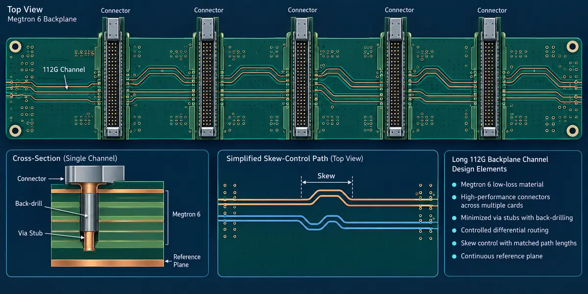
Table of Contents Channel construction Skew and weave control Via and plane continuity Coupon and release checks The released Megtron 6 PCB stackup must keep the 112G lane assumptions visible to design and fabrication. At this data rate, a small skew shift, a poorly referenced via field, or a connector launch that changes between panels...
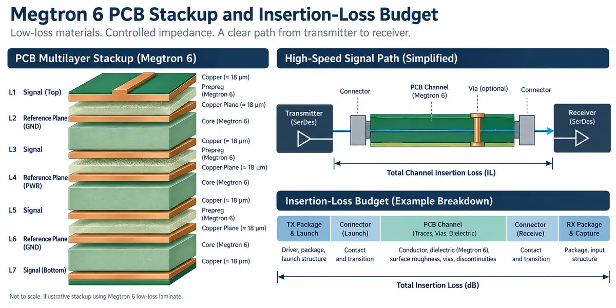
Megtron 6 PCB Material Selection: Turning Loss Budgets into a Manufacturable Stackup

Megtron 6 PCB projects often fail late for a simple reason: the electrical loss budget was written before the stackup, copper profile, and connector geometry were frozen. A material family can support demanding high-speed channels, but the released board still depends on resin content, finished dielectric thickness, reference-plane continuity, copper roughness, and fabrication capability. This...

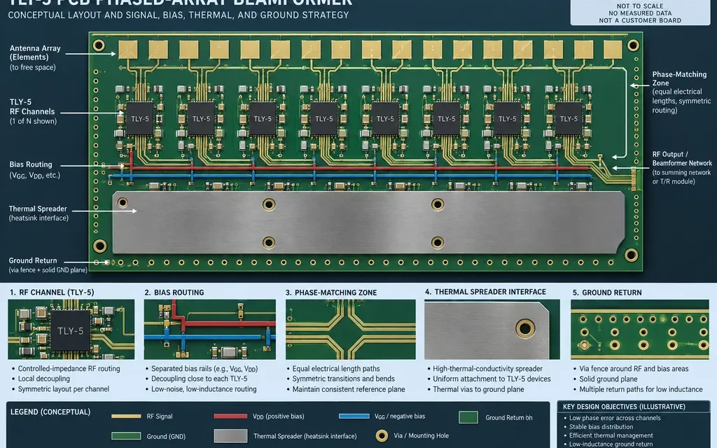
TLY-5 PCB in Phased-Array Beamformers: A Thermal and Bias-Routing Strategy

TLY-5 PCB beamformer thermal design is a coupled RF and power problem. In a phased array, each channel must preserve phase while bias networks, power amplifiers, control lines, and heat paths share a compact multilayer board. The engineering risk is not simply a hot spot; it is a hot spot that changes dielectric geometry, connector...

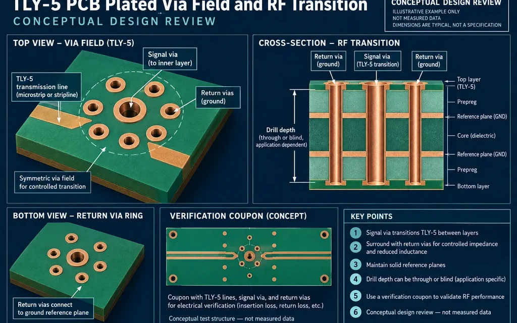
TLY-5 PCB Via Fields: Designing Plated Transitions Without Tuning Away the Real Problem

A TLY-5 PCB via field is not a cosmetic layout detail in a Ku-band module. The plated transition decides where the return current closes, how much barrel remains beyond the active layer, and whether the connector launch modeled by the RF team still represents the finished board. When this is released late, the first prototype...

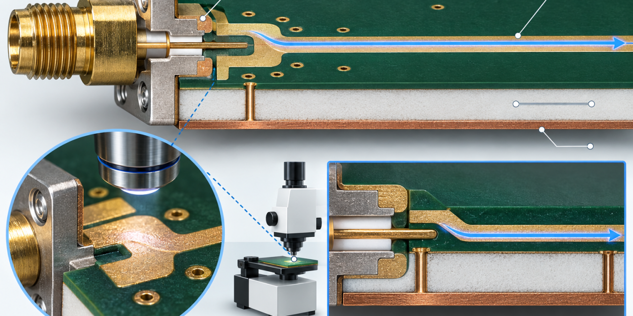
RO5880 PCB Connector Launch: 7 Critical Controls for Reliable RF Assembly

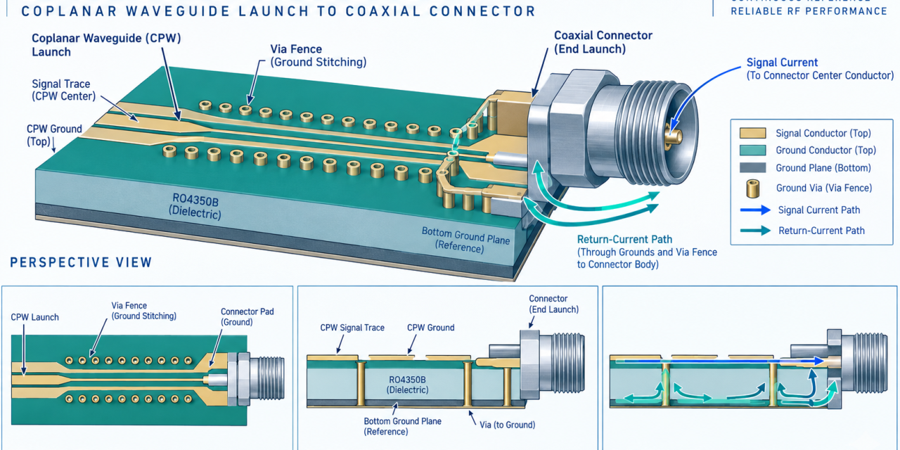
At microwave frequencies, the connector launch is often the first place where a good laminate stackup loses repeatability. The RO5880 PCB release should therefore treat the launch as a controlled subassembly. The finished RO5880 PCB must hold the launch geometry, surface finish, and reference-plane relationship while it moves through panel fabrication and assembly. This guide...

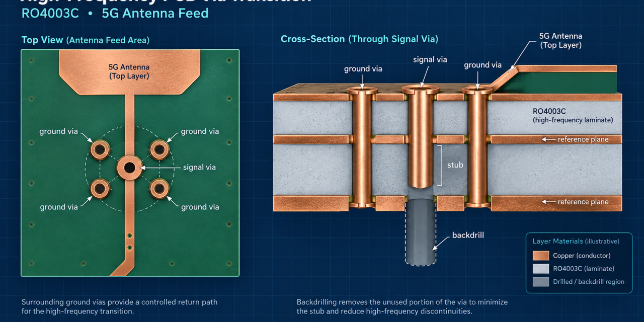
RO4350B PCB Stackup Selection for 5G and Microwave Mixed-Signal Boards

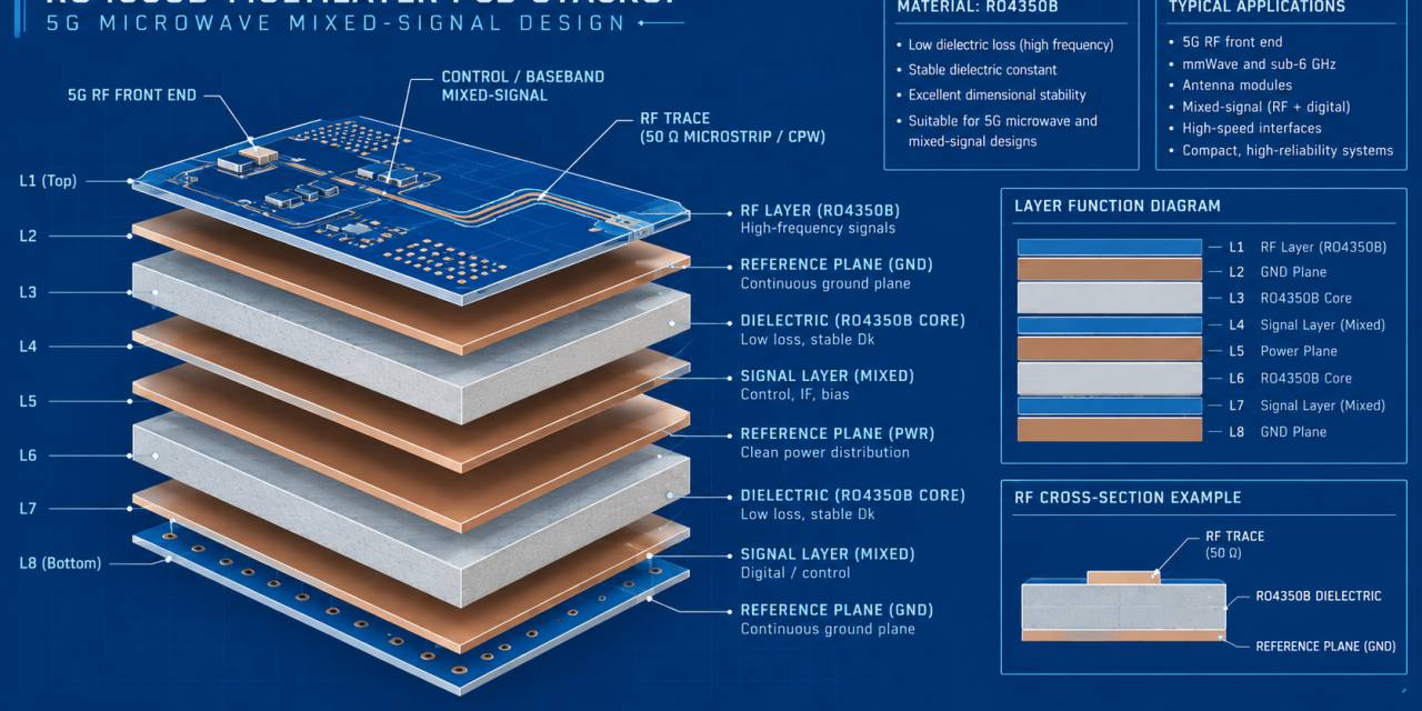
When a radio board combines a 5G front end, clock distribution, and digital processing, stackup selection becomes a system decision rather than a material shortcut. An RO4350B PCB can provide a predictable RF foundation, but only when the chosen dielectric thickness, copper, reference planes, and mixed-signal boundary are carried consistently into fabrication. This guide gives...

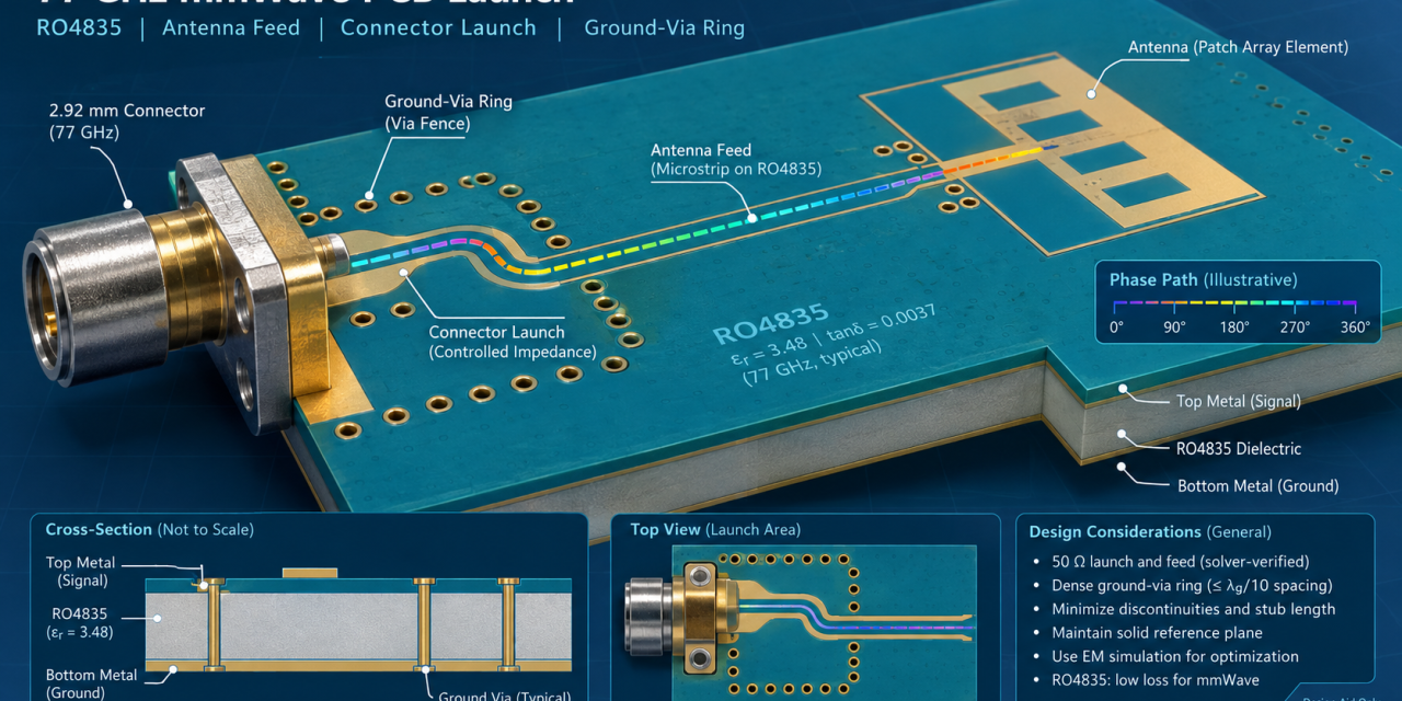
RO4835 PCB Stackup Decisions for 77 GHz Radar Phase Stability

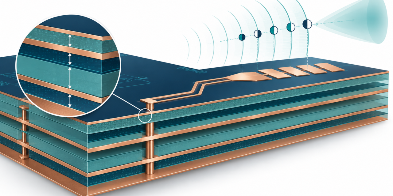
At millimeter-wave frequencies, a small dielectric or registration change can move the phase of an antenna feed enough to reduce array margin. The practical question is not simply whether an RO4835 PCB is low loss; it is how the stackup, copper geometry, and fabrication handoff keep phase repeatable from prototype to production. This engineering guide...