The Growing Demand for High Frequency Sensor PCB Technology
Modern sensing technologies are rapidly evolving toward:
- Higher operating frequencies
- Real-time signal acquisition
- Faster wireless communication
- Compact sensor integration
- Intelligent data processing
Applications such as:
- Automotive radar systems
- Industrial IoT sensors
- Aerospace monitoring equipment
- Medical imaging systems
- Smart manufacturing platforms
require highly reliable High Frequency Sensor PCB solutions capable of supporting:
- Stable RF signal transmission
- Low-loss communication
- High-speed data processing
- Precision sensing accuracy
Traditional PCB materials and layouts often struggle with:
- Signal attenuation
- Electromagnetic interference
- High-frequency transmission instability
- Sensor signal distortion
As a result, engineers increasingly adopt High Frequency Sensor PCB technology to improve:
- Sensor communication accuracy
- RF signal integrity
- Real-time sensing reliability
At KKPCB, advanced sensor PCB solutions are optimized for:
- RF sensing systems
- Microwave sensor modules
- High-speed sensor communication platforms
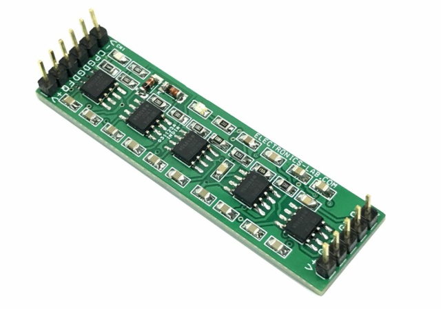
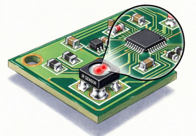
What Is a High Frequency Sensor PCB?
A High Frequency Sensor PCB is a printed circuit board specifically designed for:
- RF sensing applications
- Microwave signal detection
- High-speed sensor communication
- Precision electronic monitoring systems
These PCBs are engineered to maintain:
- Low signal loss
- Stable impedance control
- High signal integrity
- Reliable RF performance
High Frequency Sensor PCB technology is widely used in:
- Radar sensors
- Wireless sensing modules
- mmWave communication systems
- Industrial automation equipment
Key Characteristics of High Frequency Sensor PCB
Low-Loss Signal Transmission
High-frequency sensor systems require:
- Minimal insertion loss
- Stable microwave transmission
- Reduced signal attenuation
Low-loss PCB materials improve:
- Sensor detection accuracy
- RF communication stability
- Long-range sensing capability
This is especially important in:
- Automotive radar sensors
- Aerospace detection systems
- Wireless monitoring equipment
Excellent Signal Integrity
Sensor accuracy heavily depends on:
- Stable signal transmission
- Reduced RF interference
- Clean waveform propagation
High Frequency Sensor PCB design minimizes:
- Crosstalk interference
- Signal reflection
- Transmission discontinuities
- Timing distortion
These optimizations improve:
- Sensor data accuracy
- Real-time monitoring performance
- High-speed communication reliability
Controlled Impedance Routing
Controlled impedance is critical in:
- RF sensor modules
- Microwave communication systems
- High-speed sensor interfaces
Controlled impedance PCB routing improves:
- Signal consistency
- RF transmission quality
- Sensor communication stability
At KKPCB, advanced multilayer PCB optimization ensures:
- Stable impedance control
- Reliable RF signal transmission
- Better sensor communication performance
High-Density Multilayer Integration
Modern sensor systems require:
- Compact PCB layouts
- Multiple sensor interfaces
- High-speed data routing
- RF and digital signal integration
Multilayer PCB structures improve:
- Routing efficiency
- EMI suppression
- System miniaturization
- Signal isolation performance
PCB Materials for High Frequency Sensor PCB
Material selection strongly affects:
- Signal loss
- RF transmission efficiency
- Thermal stability
- Sensor reliability
Common high-frequency PCB materials include:
- Rogers RF laminates
- PTFE-based materials
- Low-loss hydrocarbon ceramic laminates
- Advanced low-loss FR4 materials
Important material properties include:
- Low dissipation factor
- Stable dielectric constant
- Excellent thermal reliability
- High-frequency electrical consistency
RF Layout Optimization in Sensor PCB Design
Proper RF PCB layout is essential for:
- Sensor precision
- Microwave transmission quality
- Stable high-frequency operation
RF layout optimization techniques include:
- Short RF routing paths
- Ground via stitching
- Smooth transmission line transitions
- Controlled return current paths
- RF shielding structures
These techniques improve:
- Sensor signal quality
- Detection reliability
- High-frequency transmission stability
EMI and EMC Optimization
High-frequency sensing systems are highly sensitive to electromagnetic interference.
EMI suppression strategies include:
- Ground shielding structures
- RF via fencing
- Layer isolation optimization
- Differential routing techniques
- Controlled return current management
Effective EMI control improves:
- Sensor accuracy
- RF stability
- Communication reliability
Thermal Management in High Frequency Sensor PCB
High-frequency sensing systems often generate heat from:
- RF processing ICs
- AI sensor processors
- Wireless communication modules
- High-speed networking chips
Thermal management solutions include:
- Thermal via arrays
- Copper heat-spreading planes
- Heat sink integration
- Multilayer thermal optimization
Efficient thermal management improves:
- Signal stability
- Sensor reliability
- Long-term operational durability
Manufacturing Challenges of High Frequency Sensor PCB
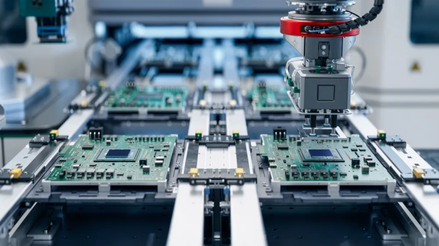
High Frequency Sensor PCB fabrication requires advanced manufacturing precision.
Key manufacturing challenges include:
- Tight impedance tolerance control
- Precision RF trace processing
- Stable dielectric thickness management
- Multilayer alignment accuracy
- Low-profile copper processing
High-frequency PCB manufacturing must minimize:
- Surface roughness variation
- Signal discontinuities
- RF transmission inconsistencies
At KKPCB, advanced PCB manufacturing technologies ensure:
- Stable electrical performance
- Reliable RF transmission quality
- Consistent multilayer PCB production capability
Applications of High Frequency Sensor PCB
High Frequency Sensor PCB technology is widely used in:
- Automotive radar sensors
- Industrial IoT systems
- Aerospace monitoring equipment
- Medical sensing systems
- Smart factory automation
- Wireless environmental sensors
- AI-powered sensing platforms
These applications require:
- Real-time signal processing
- Stable RF communication
- High-speed sensor transmission
Future Trends in High Frequency Sensor PCB Technology
Future sensor PCB development focuses on:
- mmWave sensing systems
- AI-integrated smart sensors
- Miniaturized RF sensor modules
- Ultra-low-loss multilayer PCB structures
- High-density sensor integration platforms
Emerging technologies require:
- Faster sensor communication
- Better signal integrity
- Lower RF transmission loss
- More compact sensor PCB architectures
Conclusion
High Frequency Sensor PCB technology is essential for modern:
- RF sensing systems
- Intelligent monitoring platforms
- Real-time communication electronics
Through optimized:
- Low-loss PCB materials
- Controlled impedance routing
- Signal integrity engineering
- RF multilayer stack-up design
- Advanced manufacturing precision
engineers can achieve:
- More accurate sensing capability
- Better RF communication quality
- Stable high-speed signal transmission
- Higher system reliability
With extensive expertise in RF PCB engineering and multilayer high-frequency manufacturing, KKPCB delivers advanced PCB solutions for next-generation sensing and intelligent electronic systems.
