Blog

Explore the KKPCB Blog for the latest PCB manufacturing and assembly news, industry insights, expert tips, and technology trends, helping you stay informed and optimize your electronics projects.
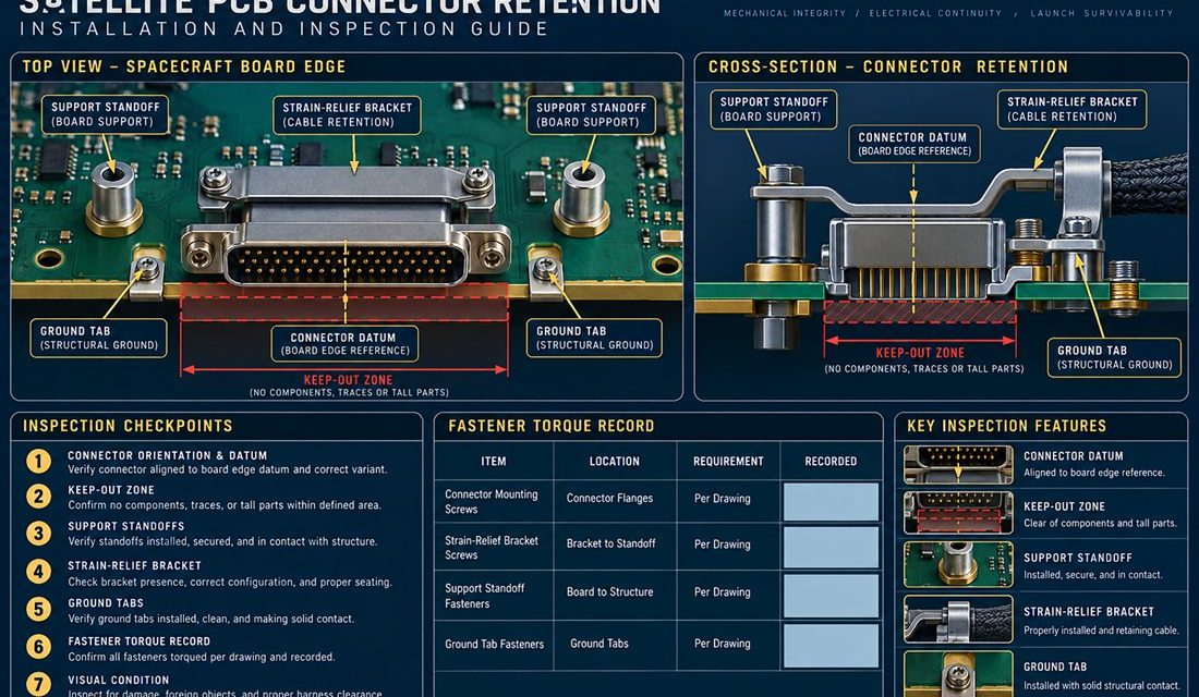
Satellite PCB Launch Vibration: Keeping Board Resonance and Connector Loads in Check

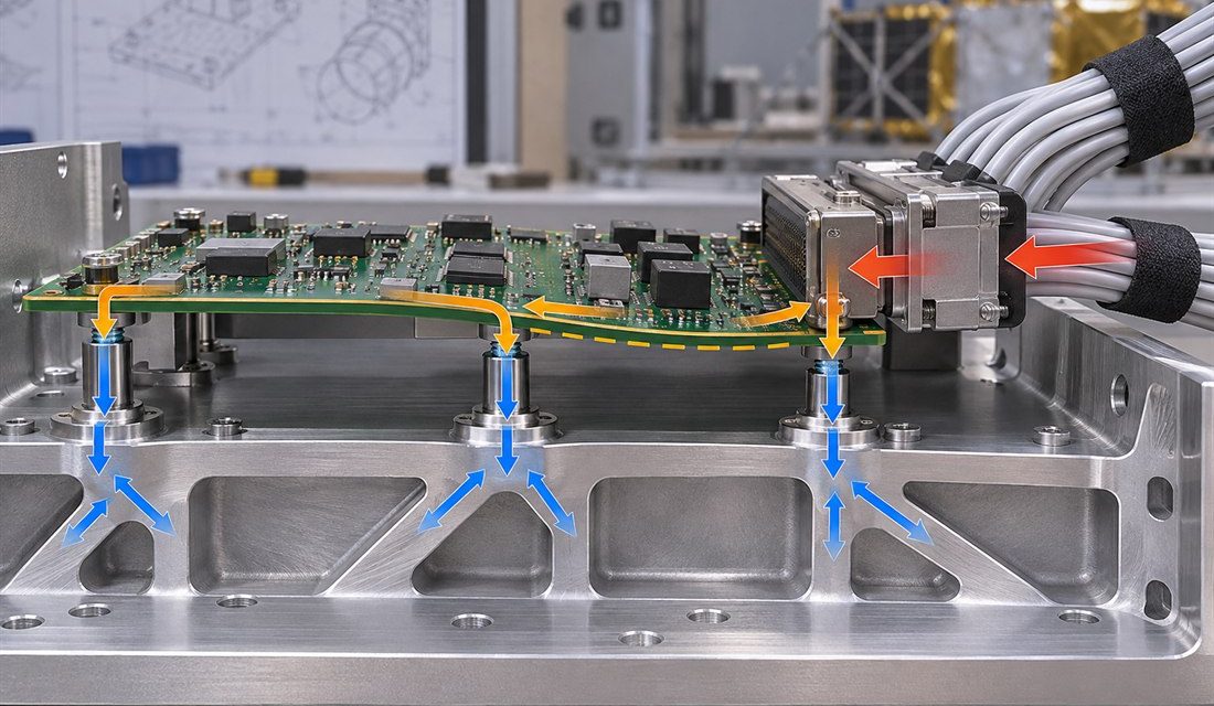
A launch environment turns a seemingly rigid electronics box into a coupled mechanical system. The spacecraft structure, chassis, mounting hardware, board, connectors, cable harness, and component masses all exchange load. If a Satellite PCB is treated as a bare laminate rather than a mounted assembly, the first resonance or a heavy connector can concentrate strain...
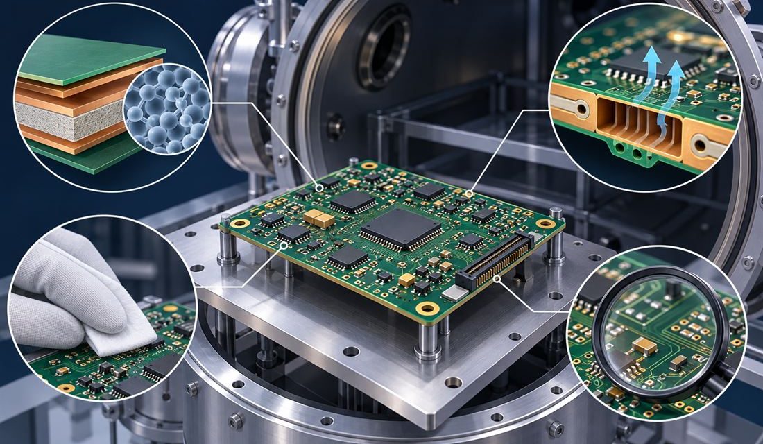

Satellite PCB Vacuum Reliability: Manage Outgassing, Cleanliness, and Material Controls

A Satellite PCB can pass electrical inspection on the bench and still become a contamination source after launch. In vacuum, volatile compounds have no convective path away from the assembly; they migrate and may condense on colder optical, RF, thermal-control, or detector surfaces. The engineering question is therefore not simply whether a laminate has a...

When EEE Parts Reach End of Life, Aerospace PCB Revision Control Matters

Aerospace PCB revision control for long-life programs begins before a substitute part reaches production. Risk appears when a component reaches end of life, procurement proposes an alternate, and the electrical design, land pattern, fabrication files, assembly instructions, and verification baseline no longer describe the same hardware. A Aerospace PCB release therefore needs a controlled change...

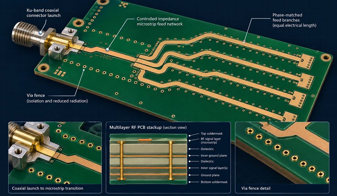
Satellite PCB Ku-Band Feed Networks: Preserving Phase Balance from Launch to Antenna

A Satellite PCB Ku-band feed network is often released as a routing problem, then fails as an integration problem. The electrical design may show equal-length branches and an acceptable nominal impedance, yet the assembled payload can lose phase balance when a connector launch, via fence, housing wall, or harness datum moves the return path. At...

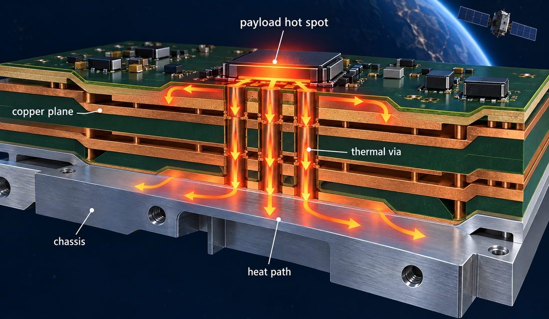
Satellite PCB Thermal Drift: Managing CTE, Copper Density, and Chassis Interfaces

Satellite PCB thermal drift becomes a mission risk when a board is treated as a flat electrical drawing instead of a constrained mechanical and thermal assembly. A payload can meet its schematic targets and still show connector strain, oscillator frequency movement, or intermittent solder fatigue after repeated hot-cold transitions. This Satellite PCB thermal drift problem...

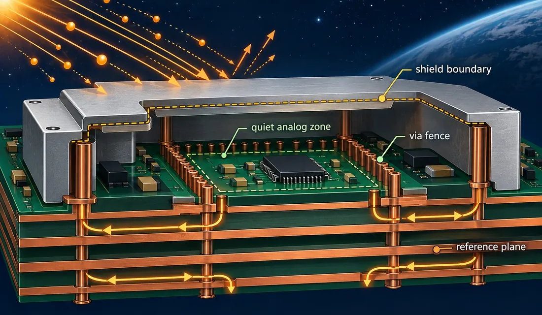
Satellite PCB Radiation Design for LEO Avionics: Dielectrics, Planes, and Shielded Returns

Satellite PCB radiation design for low-Earth-orbit avionics is often reviewed too late as a materials choice. The difficult question is not whether a board can route a signal; it is whether the dielectric, copper stack, enclosure bond, and return current still behave predictably after radiation exposure, thermal cycling, launch handling, and repeated engineering changes. A...

Ku/Ka Satellite PCB Launch Design: Taming Connector and Via Transitions at 30 GHz

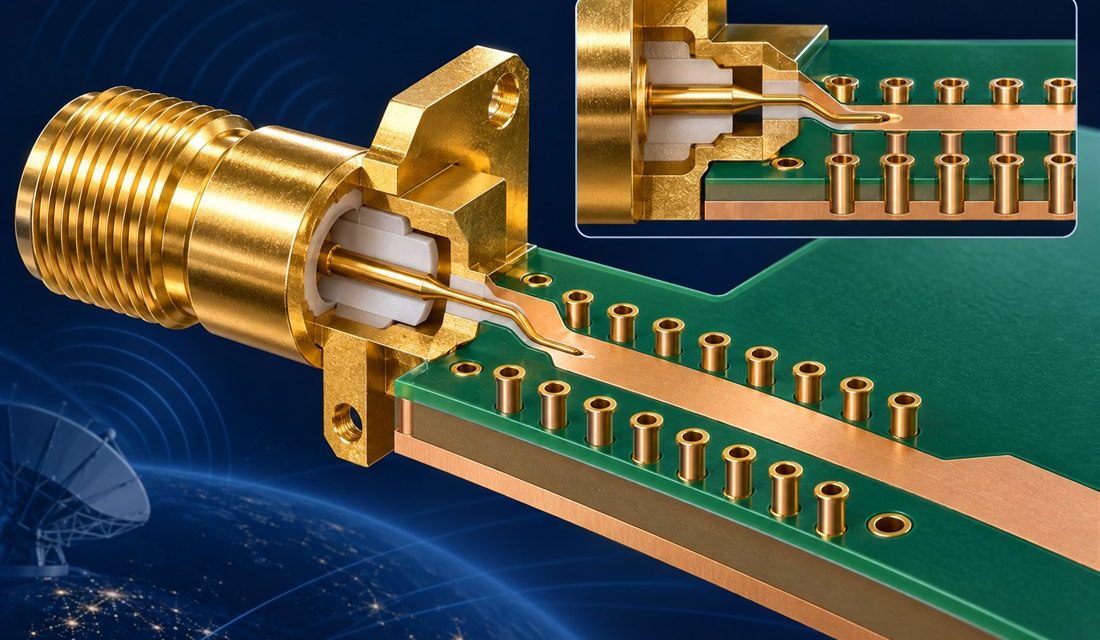
For Satellite PCB launch design, a Ku/Ka payload can meet its schematic targets and still lose margin at the board edge. The connector, launch pad, reference plane, via field, and enclosure datum form one electromagnetic interface. The Satellite PCB release must hold that board-to-enclosure datum constant across design and manufacturing. At 30 GHz, even a...

Aerospace PCB Rigid-Flex Bend Zones: Protect Copper and Connector Interfaces

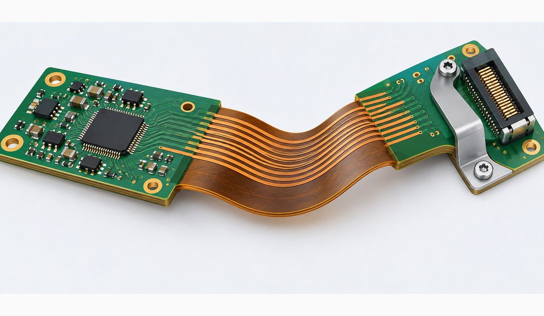
Aerospace PCB rigid-flex can remove a cable, reduce assembly volume, and simplify an avionics package, but it also moves risk into the board’s flex zone. The design can pass electrical checkout and still develop intermittent opens after deployment if the bend is treated as a packaging convenience rather than a controlled mechanical feature. For an...