
Aerospace PCB rigid-flex can remove a cable, reduce assembly volume, and simplify an avionics package, but it also moves risk into the board’s flex zone. The design can pass electrical checkout and still develop intermittent opens after deployment if the bend is treated as a packaging convenience rather than a controlled mechanical feature. For an Aerospace PCB release, the essential questions are whether the flex is static or repeatedly moving, where strain concentrates, and how connector loads reach the copper transition.
This engineering review addresses a representative flight-control or instrument module that folds during installation and remains fixed in service. It is not a customer case or a qualification claim. IPC’s rigid-flex design guidance separates bend-area conductors, neutral-axis construction, rigid-to-flex transitions, strain relief, and documentation because these are coupled decisions, not isolated drawing details. For the released interface, the Aerospace PCB plan must identify the governing standard revision and acceptance class in its procurement package.
Classify the motion before choosing the stackup
A one-time installation fold and a dynamic service loop are different design problems. Static flex is formed once or a small number of times and then restrained; dynamic flex sees repeated cycles and needs fatigue life defined against the mission profile. An Aerospace PCB drawing that says “flexible” without stating bend sequence, direction, minimum clearance, restraint points, and cycle expectation leaves manufacturing and integration teams to infer the intended use.
Start with the actual installation sequence. For an Aerospace PCB installation, does the board fold around a mandrel, close into a hinged enclosure, or flex while a technician mates the connector? Is the flex region accessible for inspection after assembly? Does a service action reopen it? Record the free-state geometry and the final constrained shape. For an Aerospace PCB, the released bend state should be inspectable after installation without moving the cable or coverlay. If repeated motion cannot be avoided, count the expected service and test cycles, include a justified margin, and validate the specific construction. Do not transfer a cable-harness life result directly to a rigid-flex PCB.
Use a rigid-flex PCB architecture only when its packaging, mass, reliability, and assembly benefits outweigh the added stackup and inspection complexity. An Aerospace PCB layout review should settle the fold datum and connector support before the artwork is frozen. Compare it with a separate cable or a conventional PCB manufacturing approach early, while the enclosure and connector positions can still change.
Keep the bend zone mechanically honest
Aerospace PCB flex strain depends on the finished construction, copper position relative to the neutral axis, bend radius, layer count, copper type and thickness, adhesive system, coverlay, and whether the bend is formed once or cycled. A generic bend-radius ratio is not a safe universal rule. Obtain the design method from the applicable IPC-2223 revision, material supplier, and fabricator; then review it against the actual cross-section and forming sequence.
Keep plated holes, component lands, stiffener edges, coverlay openings, abrupt copper-width changes, and rigid-flex interface discontinuities out of the active bend unless the selected construction and design authority explicitly allow them. Avoid routing a trace so that a narrow neck or sharp corner sits at the highest-curvature line. Where conductors must cross the bend, coordinate their direction, spacing, copper balance, and local layer arrangement with the fabricator. A nominal outline is not enough: call out the bend line, bend direction, formed radius, keep-out, and any tooling used to support forming.
The IPC-2223D table of contents specifically identifies conductors in bend areas, neutral-axis construction, reduced bend radii, rigid-flex differential lengths, strain relief, and rigid-to-flex transition considerations. Those headings are a useful review map, but the controlled standard—not a secondary summary—must govern the numerical limits. PCB layout should show the mechanical design intent alongside the electrical routing, not leave it buried in a 3D screenshot.
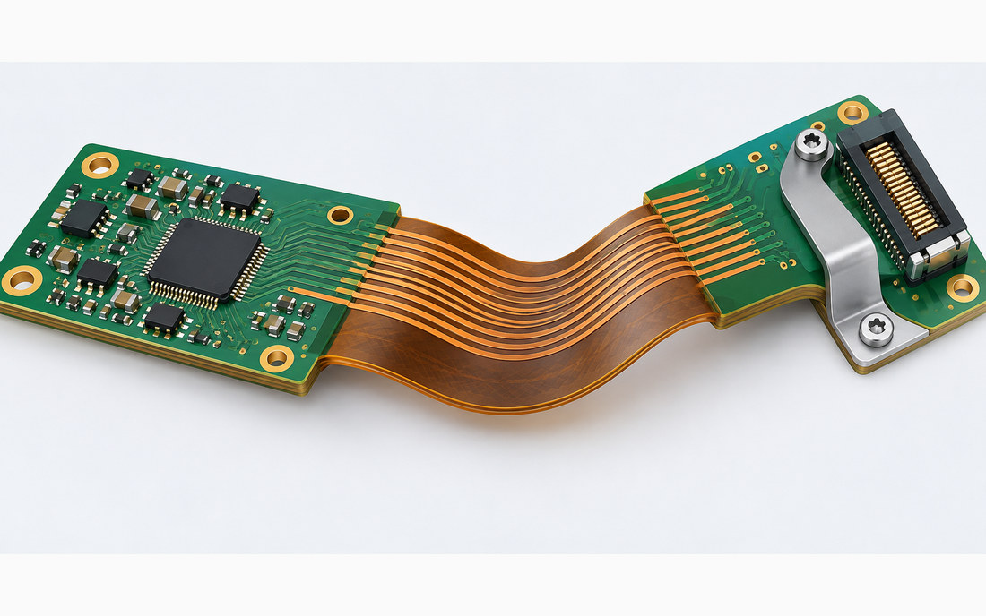
Move connector force away from the copper transition
On an Aerospace PCB, connector insertion, backshell torque, cable pull, and technician handling can load the board even when the flex itself is nominally static. If the connector sits on a rigid island, transfer its reaction force into a chassis feature, clamp, or bracket instead of allowing the flex-to-rigid boundary to act as the spring. Provide a clear mechanical datum for the connector, board support, and enclosure. Check tolerances at worst-case alignment and include the harness exit direction, bend radius, and strain-relief length.
For an edge connector or board-to-board interface, identify which side carries mating force and how it is supported during installation. For a cable connector, specify backshell support and clamp location. A connector placed too close to the transition can create peel or torsion at the coverlay edge; moving it farther away may lengthen the rigid section but improve load transfer. This is a packaging trade, so record the decision in the mechanical interface drawing and review it with electrical, mechanical, and assembly owners.
Use a suitable rigid-flex assembly plan that includes carrier support, temporary stiffening where appropriate, connector installation order, and inspection access. The PCB assembly traveler should identify whether the flex is supported during soldering, whether a connector is hand-installed or machine-placed, and how the assembly is protected from unintended re-bending.
Control the interface, not only the artwork
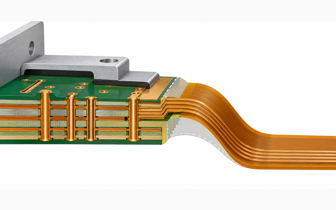
Aerospace PCB transition failures can begin with coverlay openings near a stiffener edge, abrupt thickness steps, a via too close to the rigid-flex interface, or a copper feature that becomes a local hinge. Define a transition zone with the fabricator. Review layer registration, adhesive squeeze-out, coverlay clearance, stiffener termination, copper foil type, and whether the final panelization leaves tabs or coupons that could stress the flex during separation.
The shop package for this Aerospace PCB should specify the flex and rigid stackups, materials, copper weights, coverlay, adhesive or adhesiveless construction, stiffener material and thickness, bend geometry, and finished outline. Where a flexible section contains controlled-impedance signals, treat it as a separate field-solver and validation problem: the dielectric and reference structure differ from the rigid section. A high-frequency PCB transition should not be assumed to preserve impedance simply because the trace width is unchanged. Confirm the actual cross-section with the controlled impedance capability team using the released materials and copper definition.
Agree with the fabricator on panel support and handling. Flex circuits can be damaged by sharp folds, fingernails, vacuum pickup misplacement, or unsupported connector weight. Specify protective films and removal sequence if used. Require a first-article cross-section or other agreed evidence for critical transitions, and identify the inspection method for coverlay registration and exposed copper. Do not state that a process is qualified unless the project’s own evidence establishes it.
Plan validation around failure mechanisms
For an Aerospace PCB build, verify the actual risk: continuity across the bend, insulation resistance where relevant, connector retention, visual condition after forming, and function under the defined mechanical state. If the board moves in service, define cycle count, rate, stroke, temperature, electrical monitoring, and failure criteria before testing. The Aerospace PCB verification plan should make those conditions traceable to the mission use case. For a fixed fold, validate the production forming fixture and inspect the formed assembly after the intended installation operation; repeated laboratory cycling would answer a different question.
NASA’s published dynamic flat-cable harness analysis is a useful warning about assumptions: its spacecraft instrument harness exhibited rising trace resistance and opens at about one-tenth of the planned cycle count before redesign and further analysis. That is evidence from a particular harness construction, not a rigid-flex PCB life rating or a transferable acceptance limit. It supports a project lesson: qualify the actual geometry and process, monitor resistance during cycling, and investigate the failure location rather than relying on a generic cycle claim.
Use rigid-flex design rules and the controlled board capability data as feasibility inputs, then agree on the project’s performance class, inspection level, and acceptance evidence. If a proof build is needed, a prototype assembly should preserve production-intent materials, stiffeners, connector support, and forming method; otherwise its result may not represent the released design.
Release checklist for design and program teams
- Label every flex region as static or dynamic and document the intended installation and service motion.
- Release the finished stackup, bend direction and radius, keep-out, tooling and restraint locations with the mechanical interface drawing.
- Keep connector mating forces, cable pull and backshell loads out of the flex-to-rigid transition through a defined support path.
- Review vias, lands, coverlay openings, stiffener edges, copper transitions and panelization against the bend geometry.
- Agree on representative material, cross-section, forming sequence, test conditions, cycle life if applicable, and acceptance criteria before first article.
- Track the approved drawing, fabrication data, assembly traveler, test record and concessions under the same revision baseline. The Aerospace PCB release record should identify the approved forming sequence and the responsible acceptance authority.
For an Aerospace PCB first-article review, a project manager should assign owners for the mechanical datum, electrical net review, fabrication cross-section, assembly handling, and verification record. When a supplier proposes a material or stiffener substitution for an Aerospace PCB, compare the finished neutral-axis location and transition behavior, not only nominal thickness. Treat each approved deviation as a configuration change with an impact assessment.
The practical release decision for an Aerospace PCB is to freeze the motion envelope and load path first, then finalize the stackup and bend geometry. That sequence lets electrical design, mechanical packaging, PCB fabrication and assembly work from one physical definition. It also keeps a representative engineering discussion separate from customer results, qualification claims, or guaranteed service life.
Sources: IPC-2223D, Sectional Design Standard for Flexible Printed Boards (design topics include conductors in bend areas, neutral-axis construction, rigid-flex transitions and strain relief); NASA Technical Reports Server, “Analysis of a Dynamic Flexed Flat Cable Harness,” describing a specific spacecraft instrument harness test and redesign; NASA Lessons Learned Information System, flexible harness life-test lessons. Use the revision and acceptance class specified by the project; document the Aerospace PCB transition details that apply to the released construction. The NASA harness result is not a rigid-flex PCB test result, and no KKPCB customer measurement is claimed.





