
Satellite PCB thermal drift becomes a mission risk when a board is treated as a flat electrical drawing instead of a constrained mechanical and thermal assembly. A payload can meet its schematic targets and still show connector strain, oscillator frequency movement, or intermittent solder fatigue after repeated hot-cold transitions. This Satellite PCB thermal drift problem is controlled only when the laminate, copper distribution, components, fasteners, and chassis datum are reviewed as one system. The practical question for a project team is how to keep the laminate, copper distribution, components, fasteners, and chassis datum moving together.
Where Satellite PCB thermal drift turns into a failure
Satellite PCB thermal drift is not limited to a cracked solder joint. A board can lose RF phase margin when a launch moves relative to a housing, or a precision sensor can shift when copper heat spreading changes its local temperature. In a satellite payload, the enclosure supplies the mechanical reference while the board supplies the electrical reference. If those references are not defined together, the first thermal cycle exposes a gap that was invisible during room-temperature bring-up.
Start by listing the heat sources and the constraints that cannot move. Typical sources include a DC-DC converter, FPGA, RF power amplifier, and processor. Typical constraints include coax launches, guide pins, flex tails, optical benches, and a chassis wall. Mark each item as a heat source, thermal sink, datum, or compliance feature. This map gives the layout owner a reason to reserve copper and mounting clearance instead of filling every open region with metal.
Match stack-up, copper, and CTE assumptions
A robust Satellite PCB stack-up starts with the finished board condition, not only the laminate data sheet. The project record should state dielectric family, finished dielectric thickness, copper weights, resin content, glass style, solder mask, and the expected press cycle. These values influence z-axis expansion, in-plane movement, impedance, and the amount of copper that can carry heat toward the chassis.
Use the laminate supplier’s typical data as a design input, then separate it from the acceptance limit. A typical coefficient of thermal expansion is not a promise for every press lot. The drawing should therefore identify a target range, the coupon structure, and the measurement method. If the design depends on a tight RF phase relationship, include the temperature condition for the phase or delay objective rather than quoting a room-temperature dielectric constant as if it were invariant.
For hybrid constructions, the transition between materials needs special attention. A low-loss RF core may be laminated beside a conventional digital core, while a thick copper plane spreads heat toward the housing. The interface can develop different expansion gradients during a cycle. A Satellite PCB design review should show where the hybrid boundary lies, which vias cross it, and how the connector launch is tied to the reference plane. Do not hide the boundary in a generic stack-up table.
Balance copper density before fabrication
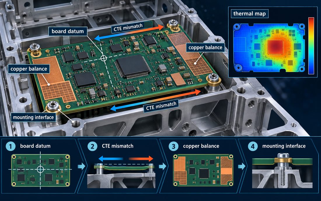
Copper balance is a mechanical control as much as an electrical one. A large copper pour on one side of a multilayer panel and a sparse region on the other can produce press-flow differences, bow, twist, or a local thickness change. Those effects become more visible when a board is screwed to a rigid chassis. The board may be forced flat during assembly, but the stored stress later appears as a lifted corner or a solder joint that sees cyclic strain.
Before releasing artwork, compare copper density by layer and by quadrant. Include plane voids, thermal reliefs, plated cavities, and large component keep-outs in the comparison. A Satellite PCB materials review should also check whether a high-copper region changes the effective dielectric thickness or the local etch compensation. These are practical questions for the fabricator because they connect the stack-up promise to the panel geometry.
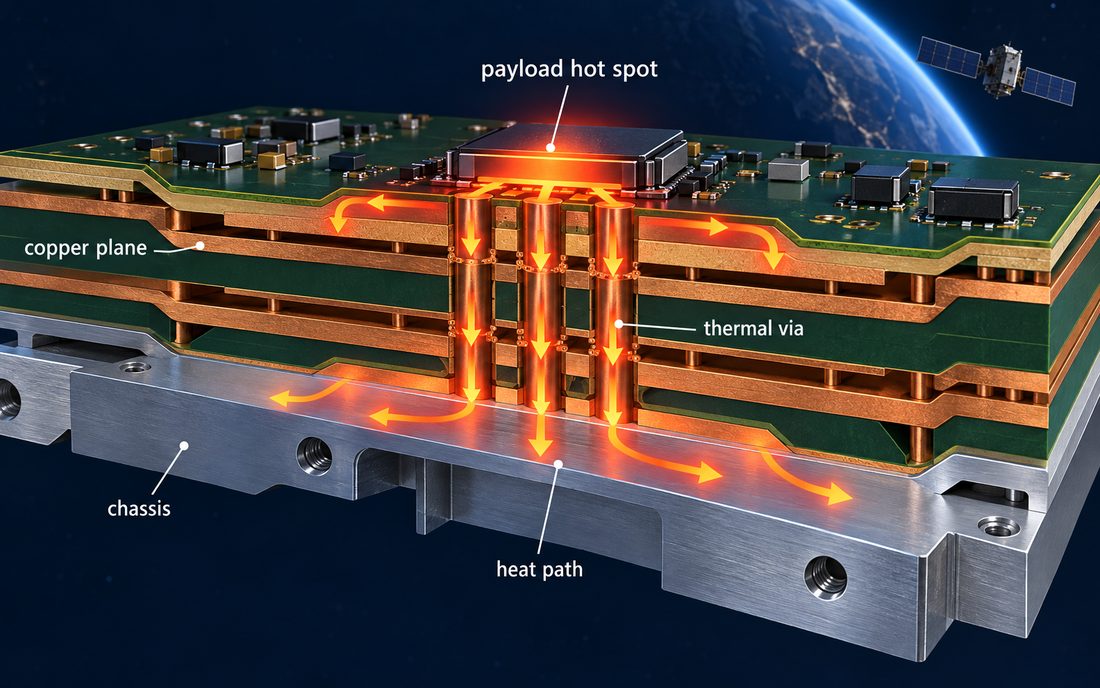
When a thermal via array is required beneath a power device, design the array as a controlled feature for Satellite PCB thermal drift control. Specify finished hole size, via pitch, solder-mask treatment, and whether the vias are filled or tented. A dense open-via field can wick solder away from an exposed pad, while an overly small pitch can reduce drill registration margin. Tie the array to the thermal plane and route the plane to the chassis interface without narrowing it at a connector cut-out.
Satellite PCB thermal drift also depends on how thermal spreading affects RF behavior. A copper island placed beneath a transmission line may change the reference geometry; a large thermal void near a launch may force the return current around the hot spot. The design owner reviewing Satellite PCB thermal drift should review thermal and RF layers together, especially when an RF power amplifier and a sensitive receiver share the same board edge.
Control chassis and connector interfaces
For Satellite PCB thermal drift, the mechanical interface is where most thermal assumptions become physical evidence. Establish a single board datum and reference every mounting hole, connector, stiffener, and shield wall to it. The Satellite PCB layout should show the datum in the drawing, in the 3D clearance model, and in the drill file notes. If a connector is positioned from a different origin than the board outline, a thermal cycle can turn a small coordinate mismatch into a large contact load.
Do not use fasteners as an unplanned heat path. If the design depends on the screw or standoff to carry heat, define the contact pad, surface finish, torque window, and interface material. If the screw is only a mechanical restraint, keep sensitive traces and vias away from the load path and provide enough clearance for thermal expansion. A rigid-flex PCB tail needs the same discipline: the bend zone, stiffener edge, and connector strain relief must be referenced to the chassis datum.
Connector launches deserve an electrical and mechanical check at the same time. Verify pad geometry, anti-pad clearance, nearby ground vias, mounting hardware, and the housing wall. A launch that is electrically correct on a free panel can be pulled out of tolerance when a bracket clamps the board. Use a representative coupon or a release vehicle with the same datum and connector stack instead of trusting an isolated coupon.
Assembly and qualification evidence
A Satellite PCB thermal drift release is not complete when the board passes visual inspection. The PCB assembly traveler should record component orientation, solder profile, cleaning method, bake condition, and inspection points around power packages, connectors, and shield cans. For high-value payload hardware, control the time between bake, assembly, cleaning, and sealed storage so that moisture and contamination do not obscure a thermal failure mode.
Require a DfMA review before qualification. Check stencil apertures above thermal pads, the rework path for a converter, the accessibility of thermocouple points, and the risk of shadowing under a shield. If a component becomes unavailable, component sourcing must flag changes in package height, thermal pad size, and power dissipation before the alternate is approved.
Use quality control evidence to tie the thermal build to the correct revision: panel identification, copper-weight records, coupon results, assembly inspection, and the torque record for chassis mounting. The evidence can support an engineering decision without being presented as a customer test result. If a qualification board is used, label the data as a design verification result for that vehicle and record the boundary conditions.
Thermal release checklist
- Define the thermal sources, sinks, board datum, and mounting constraints before final placement.
- Record stack-up, finished copper, resin, glass style, and the temperature range used for the design target.
- Compare copper density by layer and quadrant, including plane voids and via arrays.
- Review connector launches, shield walls, fasteners, and flex stiffeners in the same 3D datum.
- Release assembly profile, bake, cleaning, inspection, and rework limits with the board revision.
- Use aerospace PCB assembly controls to keep environmental evidence traceable.
- Ask for a PCB prototype that represents the intended copper, mounting, and connector geometry.
A Satellite PCB thermal release is credible when electrical, mechanical, and manufacturing assumptions are visible in one controlled package. The project manager can then decide whether a change affects only the layout, or whether it requires a new coupon, assembly build, or environmental verification step.
Sources: laminate manufacturer thermal and dimensional-stability data; NASA workmanship and contamination-control guidance; Analog Devices thermal-layout notes; Qorvo RF packaging guidance; and Würth high-frequency design references. Values are engineering targets or typical design inputs, not customer measurements.





