
Satellite PCB Power Integrity begins with the way power conversion, digital processing, RF payloads, and thermal paths share a constrained enclosure. A board may pass schematic review yet still experience rail droop during a load step, local copper heating around a connector, or reset coupling from a switching converter. A Satellite PCB power review must connect the mission load profile to the board stackup, current path, protection strategy, and test points before release.
Satellite PCB Power Integrity: Build the Load and Rail Map
Begin with an operating-mode table: startup, payload acquisition, communications transmit, processing peak, safe mode, and any simultaneous-load condition. For each state, record source voltage range, average and peak current, load-step timing, duty cycle, allowed droop, recovery requirement, and protection behavior. The NASA SmallSat power-subsystem overview describes the system-level relationships among generation, storage, and distribution; a board-level design still needs its mission-specific values and approved margins.
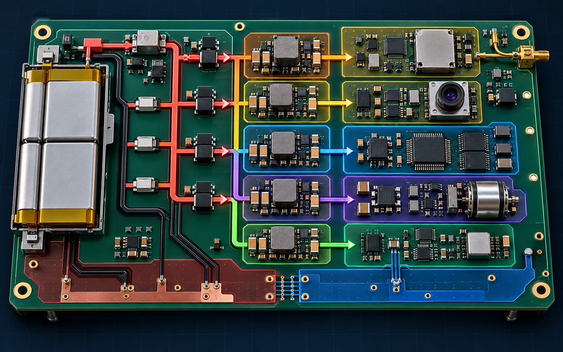
For Satellite PCB power integrity, map each branch from source connector through protection, conversion, local bulk capacitance, distribution copper, connector contacts, and load. Include return paths and sensing points rather than documenting only positive rails. A Satellite PCB power tree is easier to review when each current loop, fuse or switch, telemetry point, and isolated domain appears on one drawing. This prevents a layout team from discovering late that a “quiet” sensor supply shares copper or return impedance with a high-pulse transmitter load. Include the return-plane construction in this same rail map when the payload includes sensitive RF paths.
Satellite PCB Power Integrity: Size copper from the full thermal path
Estimate conductor loss using the released copper thickness, width, length, and expected current profile, then check the thermal path through adjacent copper, vias, laminate, mounting points, and enclosure. A trace-width calculator alone cannot account for connector contact resistance, constrictions, via arrays, plane neck-downs, nearby heat sources, airflow assumptions, or vacuum operation. Treat calculated temperature rise as an engineering estimate with declared boundary conditions; it is not a board measurement or a qualification result.
Review where current enters and leaves large planes, whether the return path stays continuous, and whether current crowds around a clearance or slot. Check copper balance and local copper density so that the power feature does not create avoidable etching, registration, or flatness risk. The PCB manufacturing release should specify copper weight, finished thickness, finished hole requirements, and any controlled geometry that materially affects resistance. If the design uses high-current vias, document the via construction and ensure the expected current is distributed across the intended barrels rather than assumed to divide uniformly. A multilayer PCB construction review should confirm that the selected via structure is compatible with the released stackup.
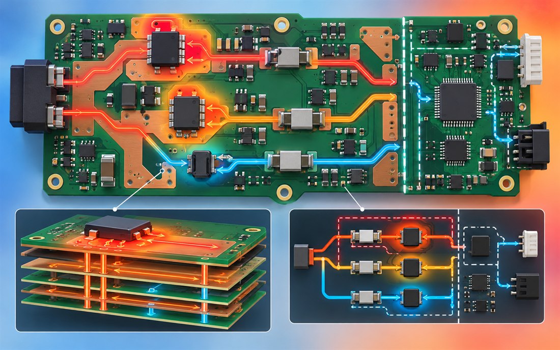
For Satellite PCB Power Integrity, thermal analysis should reflect the actual mounting and dissipation boundary; this is part of SmallSat power integrity, not a separate cosmetic check. A vacuum enclosure removes convective cooling, so the heat path may depend strongly on copper spreading, interface materials, chassis contact, and component placement. Do not promise a temperature from a generic material value; identify which values are supplier typical data, model assumptions, design limits, or measured conditions. A Satellite PCB design review should flag any missing thermal boundary condition before the team approves copper or component derating.
Satellite PCB Power Integrity: Separate noisy conversion from sensitive loads
Satellite PCB Power Integrity can be compromised when switching converters and pulsed loads disturb sensitive analog or RF circuits through conducted noise, shared return impedance, magnetic coupling, or poor sequencing. Place the converter input loop compactly, keep the switch node away from sensitive inputs, and provide a clear return path to the source. Separate domains only when the schematic and system architecture define where they connect; an arbitrary split plane can force return current into a longer path and create new coupling.
Review regulator stability with the selected capacitor technology, effective capacitance under bias, ESR and ESL, layout parasitics, and load-step envelope. Verify enable sequencing and startup current against the source and protection device. Decoupling values should come from regulator and payload requirements, not from a generic “more capacitance is better” rule. The Satellite PCB layout should preserve sensitive reference nodes and avoid routing their feedback or current-sense traces alongside a fast switch node.
For a mixed-signal board, establish the return-current path for every critical interface and ensure ADC references, telemetry dividers, current shunts, and reset signals observe the intended rail. The PCB layout and PCB assembly teams should also agree on probe access and rework limits. A current-sense element placed in the wrong branch can make a robust protection circuit appear ineffective during bring-up. Use a connector assembly review to confirm that the selected load interface can be inspected and mechanically supported.
Satellite PCB Power Integrity: Design fault containment and verification
For Satellite PCB Power Integrity, define the fault response for each rail: overcurrent, short circuit, undervoltage, converter loss, reverse current, and failed telemetry. Decide what is latched, what can retry, what must be isolated, and which loads are shed first. A protection device selected only by nominal current may nuisance-trip on startup or fail to limit a fault quickly enough. Coordinate threshold, response time, thermal dissipation, component tolerance, and expected source impedance with the power-system owner.
Test a staged Satellite PCB Power Integrity design with current-limited supplies and representative loads. For Satellite PCB Power Integrity verification, capture input and output waveforms at the board connector and at the point of load; include probe ground strategy and bandwidth limits in the record. Exercise startup, load steps, mode changes, and fault injection only within the approved test procedure. Compare measurements against the released design limits and preserve the hardware revision, BOM, firmware mode, fixture, and ambient or thermal-vacuum conditions. A prototype assembly is useful for learning only if the test setup and board configuration are traceable.
Satellite PCB Power Integrity manufacturing checks complement but do not replace electrical validation. Inspect high-current connector joints, via fields, solder coverage, polarity, component identity, and the copper features that carry the critical load. The SMT assembly plan should record approved alternates and reflow requirements for the power components. Any change to capacitor series, regulator package, copper thickness, or connector source requires review of stability, thermal, and protection assumptions.
Satellite PCB Power Integrity: Close the production handoff
For Satellite PCB Power Integrity release, align the schematic, native PCB data, stackup, power-tree drawing, BOM, fabrication notes, assembly instructions, and verification plan. Mark controlled alternates and the approval authority for each. Define what the supplier may clarify and what requires written design-authority approval. This prevents an emergency component substitution or copper change from silently altering a current path after the qualification baseline was established.
- Document operating modes, source range, peak and average loads, allowed droop, and recovery behavior.
- Check each power and return path for resistance, thermal spreading, via construction, connector loss, and manufacturability.
- Review switching loops, sensitive nodes, sensing locations, sequencing, and domain boundaries.
- Define fault protection, safe-state behavior, and approved fault-injection limits.
- Specify test points, fixtures, measurement bandwidth, acceptance limits, and configuration records.
- Control copper, stackup, component, supplier, and firmware changes through an impact review.
In a Satellite PCB Power Integrity review, a project manager can use this checklist to separate unresolved electrical risk from fabrication data gaps and test dependencies. A Satellite PCB power release is strongest when assumptions are visible, limits are approved, and the same revision is used by design, sourcing, assembly, and verification. Where an early validation lot is needed, a prototype build can check the defined interfaces without being presented as mission qualification. Align the fabrication data package with the same controlled electrical baseline. High-current routing and heat-spreading decisions should be confirmed before procurement rather than after a schedule-critical prototype has been built.
Sources: NASA Small Spacecraft Systems Virtual Institute, “Power Subsystems”; NASA-HDBK-4001A, spacecraft electrical grounding and bonding guidance. These sources provide system-level context; no mission-specific load profile, temperature measurement, or KKPCB test result is asserted.





