HomeTag

panelization - KKPCB

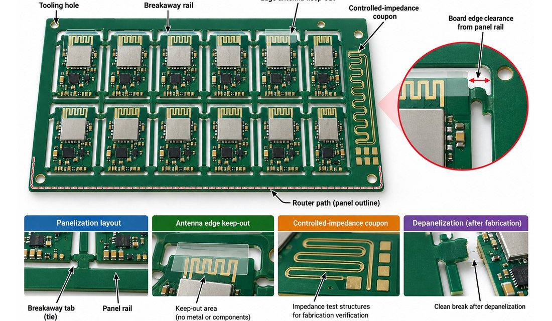
Why a Zigbee PCB Passes Layout Review but Fails at Panelization

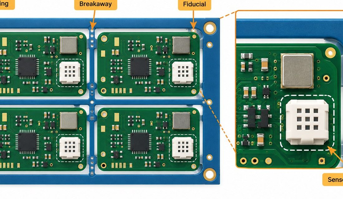
Table of Contents Treat the panel as an RF state Protect the antenna edge and return path Control tabs, rails, and depanelization Release evidence for assembly and test A Zigbee PCB can pass a single-board layout review and still lose repeatability when it enters a manufacturing panel. Breakaway rails, tooling holes, router paths, copper balance,...

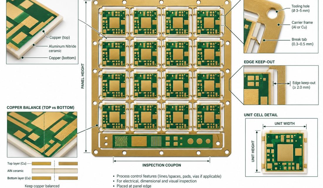
Aluminum Nitride PCB Inverter Modules: DFM, Panel Handling, and Production Release Controls

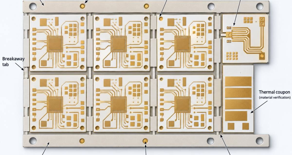
An Aluminum Nitride PCB inverter module release should connect panel handling, copper interfaces, and inspection evidence before production volume is authorized. Inverter modules expose the difference between a ceramic concept and a repeatable production process. Heavy copper, AlN substrate, switching devices, isolation clearances, carrier support, and inspection access all compete for the same panel area....

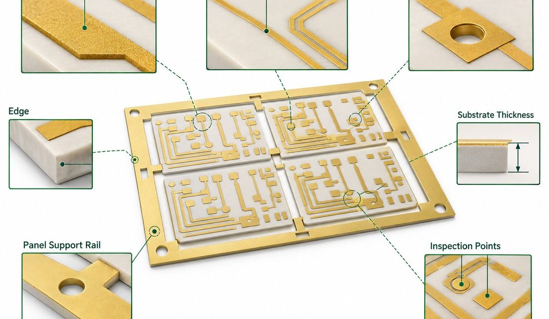
Alumina PCB DFM: Metallization, Panel Handling, and Inspection Before Volume Release

Volume release exposes the difference between a ceramic layout and a ceramic process. Screen, thick-film, thin-film, plated, brazed, and bonded features each have a different capability window. An Alumina PCB drawing that specifies only line widths and hole sizes can still leave the supplier guessing about paste, firing, edge handling, carrier support, and inspection. The...

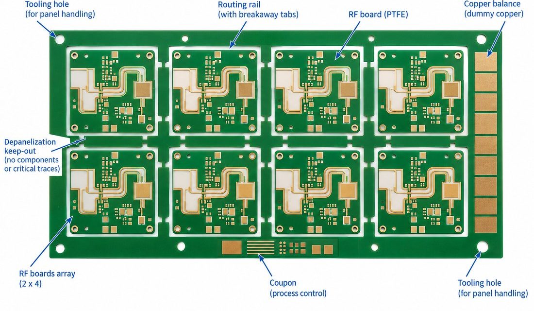
PTFE PCB DFM: Panelization and Procurement Controls for Repeatable RF Builds

A PTFE board can be electrically well designed and still be difficult to quote or panelize. The manufacturing risk is concentrated at the interfaces: copper balance, drilled features, plated edges, hybrid stackup boundaries, connector rails, and the coupon that is supposed to represent the RF path. A PTFE PCB release should therefore explain the process...

Ceramic PCB DFM and Procurement Release: Avoiding First-Build Surprises

Ceramic PCB programs often move from concept to purchase order faster than the manufacturing package matures. The layout may be complete, but the supplier still lacks a defined panel, edge condition, metallization note, inspection plan, or approved substitute rule. That gap creates schedule risk because a ceramic panel is not interchangeable with a conventional laminate...

Megtron 7 PCB DFM Release: Panelization, Coupons, and ECO Control Before Volume Build

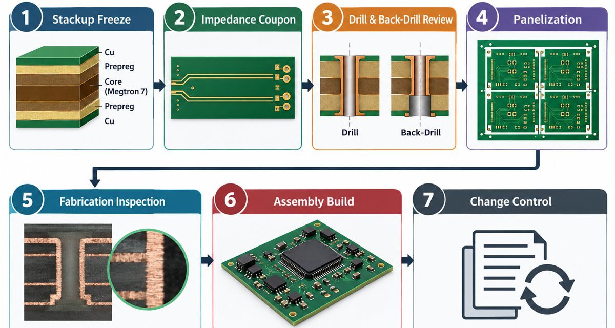
The most expensive Megtron 7 PCB problem is often a release problem, not a material problem. A prototype may route correctly, yet the volume panel has no representative coupon, uneven copper, an impractical depanelization rail, or an ECO that quietly changes the impedance construction. A useful DFM gate turns the electrical intent into a package...